SNVSBF5C July 2019 – May 2020 LP3470A
PRODUCTION DATA.
- 1 Features
- 2 Applications
- 3 Description
- 4 Revision History
- 5 Device Comparison Table
- 6 Pin Configuration and Functions
- 7 Specifications
- 8 Detailed Description
- 9 Application and Implementation
- 10Power Supply Recommendations
- 11Layout
- 12Device and Documentation Support
- 13Mechanical, Packaging, and Orderable Information
Package Options
Mechanical Data (Package|Pins)
- DBV|5
Thermal pad, mechanical data (Package|Pins)
Orderable Information
8.3.2 RESET Output
In applications like microprocessor (µP) systems, errors might occur in system operation during power up, power down, or brownout conditions. It is imperative to monitor the power supply voltage to prevent these errors from occurring.
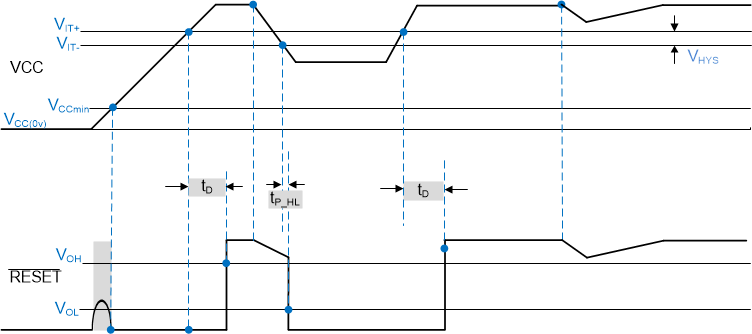
The LP3470A asserts a reset signal whenever the VCC supply voltage is below a threshold (VIT-) voltage. RESET is ensured to be a logic low for VCC > 0.95 V. Once VCC exceeds the reset threshold plus a hysteresis voltage, the reset is kept asserted for a time period (tD) programmed by an external capacitor (CSRT); after this interval RESET goes to logic high. If a brownout condition occurs (monitored voltage falls below the reset threshold), RESET goes low. When VCC returns above the reset threshold plus a hysteresis voltage, RESET remains low for a time period tD before going to logic high. Figure 9 shows this behavior.
 Figure 9. RESET Output Timing Diagram