SNOSCT6F March 2013 – January 2017 LP38798
PRODUCTION DATA.
- 1 Features
- 2 Applications
- 3 Description
- 4 Revision History
- 5 Pin Configuration and Functions
- 6 Specifications
- 7 Detailed Description
- 8 Application and Implementation
- 9 Power Supply Recommendations
- 10Layout
- 11Device and Documentation Support
- 12Mechanical, Packaging, and Orderable Information
Package Options
Mechanical Data (Package|Pins)
- DNT|12
Thermal pad, mechanical data (Package|Pins)
Orderable Information
10 Layout
10.1 Layout Guidelines
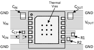
The dynamic performance of the LP38798 is dependant on the layout of the PCB. PCB layout practices that are adequate for typical LDOs may degrade the PSRR, noise, or transient performance of the LP38798.
Best performance is achieved by placing all of the components on the same side of the PCB as the LP38798, and as close as is practical to the LP38798 package. All component ground connections must be back to the LP38798 analog ground connection using as wide and short of a copper trace as is practical. The connection from the FB pin to the VSET resistors must be as short as possible as the FB pin is a high impedance input. Any trace length on the FB pin acts as an antenna.
Connections using long trace lengths, narrow trace widths; avoid connections through vias, which add parasitic inductances and resistance that results in inferior performance especially during transient conditions.
A ground plane, either on the opposite side of a two-layer PCB, or embedded in a multi-layer PCB, is strongly recommended. This Ground Plane serves two purposes :
- Provides a circuit reference plane to assure accuracy, and
- Provides a thermal plane to remove heat from the LP38798 through thermal vias under the package DAP.
10.2 Layout Example

10.3 Thermal Considerations
The value of RθJA for the 12-lead WSON package is specifically dependent on PCB copper area, copper thickness, the number of layers, and thermal vias under the exposed thermal pad (DAP). Refer to A Guide to Board Layout for Best Thermal Resistance for Exposed Packages for general guidelines for mounting packages with exposed thermal pads.
Exceeding the maximum allowable power dissipation defined by the final RθJA will cause excessive die temperature, and the regulator may go into thermal shutdown.
10.4 Estimating the Junction Temperature
The EIA/JEDEC standard (JESD51-2) provides methodologies to estimate the junction temperature from external measurements (ΨJB references the temperature at the PCB, and ΨJT references the temperature at the top surface of the package) when operating under steady-state power dissipation conditions. These methodologies have been determined to be relatively independent of the copper thermal spreading area that may be attached to the package DAP when compared to the more typical RθJA. Refer to Semiconductor and IC Package Thermal Metrics, for specifics.