SNOSCT6F March 2013 – January 2017 LP38798
PRODUCTION DATA.
- 1 Features
- 2 Applications
- 3 Description
- 4 Revision History
- 5 Pin Configuration and Functions
- 6 Specifications
- 7 Detailed Description
- 8 Application and Implementation
- 9 Power Supply Recommendations
- 10Layout
- 11Device and Documentation Support
- 12Mechanical, Packaging, and Orderable Information
Package Options
Mechanical Data (Package|Pins)
- DNT|12
Thermal pad, mechanical data (Package|Pins)
Orderable Information
5 Pin Configuration and Functions
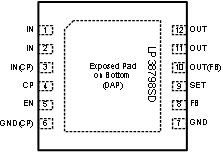
DNT Package
12-Pin WSON
Top View

Connect WSON DAP to GND at Pins 6 and 7.
Pin Functions
| PIN | I/O | DESCRIPTION | |
|---|---|---|---|
| NUMBER | NAME | ||
| 1, 2 | IN | I | Device unregulated input voltage pins. Connect pins together at the package. |
| 3 | IN(CP) | I | Charge pump input voltage pin. Connect directly to pins 1 and 2 at the package. |
| 4 | CP | O | Charge pump output. See Charge Pump section in Application and Implementation for more information. |
| 5 | EN | I | Enable pin. This pin has an internal pullup to turn the LDO output on by default. A logic low level turns the LDO output Off, and reduce the operating current of the device. See Enable Input Operation section in Application and Implementation for more information. |
| 6 | GND(CP) | — | Device charge pump ground pin. |
| 7 | GND | — | Device analog ground pin. |
| 8 | FB | i | Feedback pin for programming the output voltage. |
| 9 | SET | I/O | Reference voltage output, and noise filter input. A feedback resistor divider network from this pin to FB and GND will set the output voltage of the device. |
| 10 | OUT(FB) | I | OUT buffer feedback input pin. Connect directly to pins 11 and 12 at the package. |
| 11, 12 | OUT | O | Device regulated output voltage pins. Connect pins together at the package. |
| Exposed Pad | DAP | — | The exposed die attach pad on the bottom of the package must be connected to a copper thermal pad on the PCB at ground potential. Connect to ground potential or leave floating. Do not connect to any potential other than the same ground potential seen at device pins 6 (GND(CP)) and 7 (GND). See Thermal Considerations section in Layout for more information. |