SNVS159H October 2001 – July 2015 LP3981
PRODUCTION DATA.
- 1 Features
- 2 Applications
- 3 Description
- 4 Revision History
- 5 Pin Configuration and Functions
- 6 Specifications
- 7 Parameter Measurement Information
- 8 Detailed Description
- 9 Application and Implementation
- 10Power Supply Recommendations
- 11Layout
- 12Device and Documentation Support
- 13Mechanical, Packaging, and Orderable Information
Package Options
Mechanical Data (Package|Pins)
Thermal pad, mechanical data (Package|Pins)
Orderable Information
1 Features
- 2.5-V to 6-V Input Range
- 300-mA Output Current
- 60-dB PSRR at 1 kHz
- ≤ 1-μA Quiescent Current When Shut Down
- Fast Turnon Time: 120 μs (typical) with CBYPASS = 0.01 µF
- 132-mV Typical Dropout with 300-mA Load
- 35-μVrms Output Noise Over 10 Hz to 100 kHz
- Logic Controlled Enable
- Stable With Ceramic and High-Quality Tantalum Capacitors
- Thermal Shutdown and Short-Circuit Current Limit
- Low Thermal Resistance in WSON-6 Package Gives Excellent Power Capability
2 Applications
- CDMA Cellular Handsets
- Wideband CDMA Cellular Handsets
- GSM Cellular Handsets
- Portable Information Appliances
3 Description
Performance of the LP3981 device is optimized for battery-powered systems to deliver ultra-low-noise, extremely low dropout voltage, and low quiescent current. Regulator ground current increases only slightly in dropout, further prolonging the battery life.
Power supply rejection is better than 60 dB at low frequencies. This high power supply rejection is maintained down to lower input voltage levels common to battery-operated circuits.
The device is ideal for mobile phone and similar battery-powered wireless applications. It provides up to 300 mA, from a 2.5-V to 6-V input, consuming less than 1 µA in disable mode.
The LP3981 is available in 8-pin VSSOP-8 and 6-pin WSON packages. Performance is specified for −40°C to +125°C temperature range. The device available in the following output voltages: 2.5 V, 2.7 V, 2.8 V, 2.83 V, 3 V, 3.03 V and 3.3 V as standard. Other output options can be made available; contact your local TI sales office for more information.
Device Information(1)
| PART NUMBER | PACKAGE | BODY SIZE (NOM) |
|---|---|---|
| LP3981 | WSON (6) | 4.00 mm x 3.00 mm |
| VSSOP (8) | 3.00 mm x 3.00 mm |
- For all available packages, see the orderable addendum at the end of the data sheet.
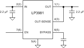
Typical Application Circuit
