SNVS441I January 2007 – November 2016 LP5521
PRODUCTION DATA.
- 1 Features
- 2 Applications
- 3 Description
- 4 Revision History
- 5 Pin Configuration and Functions
-
6 Specifications
- 6.1 Absolute Maximum Ratings
- 6.2 ESD Ratings
- 6.3 Recommended Operating Conditions
- 6.4 Thermal Information
- 6.5 Electrical Characteristics
- 6.6 Charge Pump Electrical Characteristics
- 6.7 LED Driver Electrical Characteristics (R, G, B Outputs)
- 6.8 Logic Interface Characteristics
- 6.9 I2C Timing Requirements (SDA, SCL)
- 6.10 Typical Characteristics
-
7 Detailed Description
- 7.1 Overview
- 7.2 Functional Block Diagram
- 7.3 Feature Description
- 7.4 Device Functional Modes
- 7.5 Programming
- 7.6
Register Maps
- 7.6.1 Enable Register (Enable)
- 7.6.2 Operation Mode Register (OP Mode)
- 7.6.3 R Channel PWM Control (R_PWM)
- 7.6.4 G Channel PWM Control (G_PWM)
- 7.6.5 B Channel PWM Control (B_PWM)
- 7.6.6 R Channel Current (R_CURRENT)
- 7.6.7 G Channel Current (G_CURRENT)
- 7.6.8 B Channel Current (B_CURRENT)
- 7.6.9 Configuration Control (CONFIG)
- 7.6.10 R Channel Program Counter Value (R Channel PC)
- 7.6.11 G Channel Program Counter Value (G Channel PC)
- 7.6.12 B Channel Program Counter Value (B Channel PC)
- 7.6.13 Status/Interrupt Register
- 7.6.14 RESET Register
- 7.6.15 GPO Register
- 7.6.16 Program Memory
- 8 Application and Implementation
- 9 Power Supply Recommendations
- 10Layout
- 11Device and Documentation Support
- 12Mechanical, Packaging, and Orderable Information
Package Options
Mechanical Data (Package|Pins)
Thermal pad, mechanical data (Package|Pins)
Orderable Information
8 Application and Implementation
NOTE
Information in the following applications sections is not part of the TI component specification, and TI does not warrant its accuracy or completeness. TI’s customers are responsible for determining suitability of components for their purposes. Customers should validate and test their design implementation to confirm system functionality.
8.1 Application Information
The LP5521 is designed as a autonomous lighting controller for mobile devices. These devices need extremely small form factor; therefore, the LP5521 is designed to require only 4 small capacitors: input, output, and two fly-capacitors for charge pump. If charge pump is not needed in the application (input voltage is high enough for driving LEDs), the charge pump capacitors can be omitted thus reducing the solution size even further. LED can be RGB LED or any color if desired.
8.2 Typical Applications
Application with Charge Pump shows an example of typical application which uses charge pump to get high enough voltage to drive LEDs. The device is powered from single Li-Ion battery with voltage range of 2.7 V to 4.2 V.
8.2.1 Application with Charge Pump
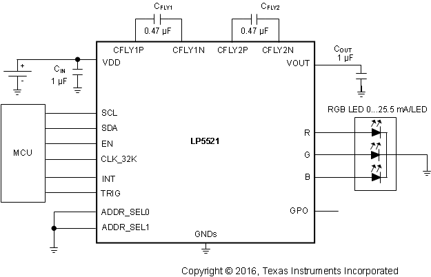 Figure 26. LP5521 Typical Application Schematic With Charge Pump
8.2.1.1 Design Requirements
| DESIGN PARAMETER | EXAMPLE VALUE |
|---|---|
| Input voltage range | 2.7 V to 4.2 V (single Li-Ion cell battery) |
| LED VF (maximum) | 3.6 V |
| LED current | 25.5 mA maximum |
| Input capacitor | CIN = 1 μF |
| Output capacitor | COUT = 1 μF |
| Fly capacitors | CFLY1 = CFLY2 = 470 nF |
| Charge pump mode | Automatic or 1.5× |
8.2.1.2 Detailed Design Procedure
8.2.1.2.1 Capacitor Selection
The LP5521 requires 4 external capacitors for proper operation (CIN = COUT = 1 μF, CFLY1 = CFLY2 = 470 nF). Surface-mount multi-layer ceramic capacitors are recommended. These capacitors are small, inexpensive and have very low equivalent series resistance (ESR < 20 mΩ typical). Tantalum capacitors, OS-CON capacitors, and aluminum electrolytic capacitors are not recommended for use with the LP5521 due to their high ESR, as compared to ceramic capacitors.
For most applications, ceramic capacitors with X7R or X5R temperature characteristic are preferred for use with the LP5521. These capacitors have tight capacitance tolerance (as good as ±10%) and hold their value over temperature (X7R: ±15% over –55°C to 125°C; X5R: ±15% over –55°C to 85°C).
Capacitors with Y5V or Z5U temperature characteristic are generally not recommended for use with the LP5521. Capacitors with these temperature characteristics typically have wide capacitance tolerance (+80%, –20%) and vary significantly over temperature (Y5V: +22%, –82% over –30°C to +85°C range; Z5U: +22%, –56% over +10°C to +85°C range). Under some conditions, a nominal 1-μF Y5V or Z5U capacitor could have a capacitance of only 0.1 μF. Such detrimental deviation is likely to cause Y5V and Z5U capacitors to fail to meet the minimum capacitance requirements of the LP5521.
The minimum voltage rating acceptable for all capacitors is 6.3 V. The recommended voltage rating of the output capacitor is 10 V to account for DC bias capacitance losses.
NOTE
Some ceramic capacitors, especially those in small packages, exhibit a strong capacitance reduction with the increased applied voltage (DC bias effect). The capacitance value can fall below half of the nominal capacitance. Choose output and input capacitor with DC bias voltage effect better than –50% at 5 V voltage (0.5 μF at 5 V).
Table 36. External Component Examples
| MODEL | TYPE | VENDOR | VOLTAGE RATING | SIZE INCH (mm) |
|---|---|---|---|---|
| 1 μF for COUT and CIN | ||||
| C1005X5R1A105K | Ceramic X5R | TDK | 10 V | 0402 (1005) |
| ECJ0EB1A105M | Ceramic X5R | Panasonic | 10 V | 0402 (1005) |
| ECJUVBPA105M | Ceramic X5R, array of two | Panasonic | 10 V | 0504 |
| 470 nF for CFLY1-2 | ||||
| C1005X5R1A474K | Ceramic X5R | TDK | 10 V | 0402 (1005) |
| ECJ0EB0J474K | Ceramic X5R | Panasonic | 10 V | 0402 (1005) |
| LEDs | User Defined | |||
8.2.1.3 Application Curves
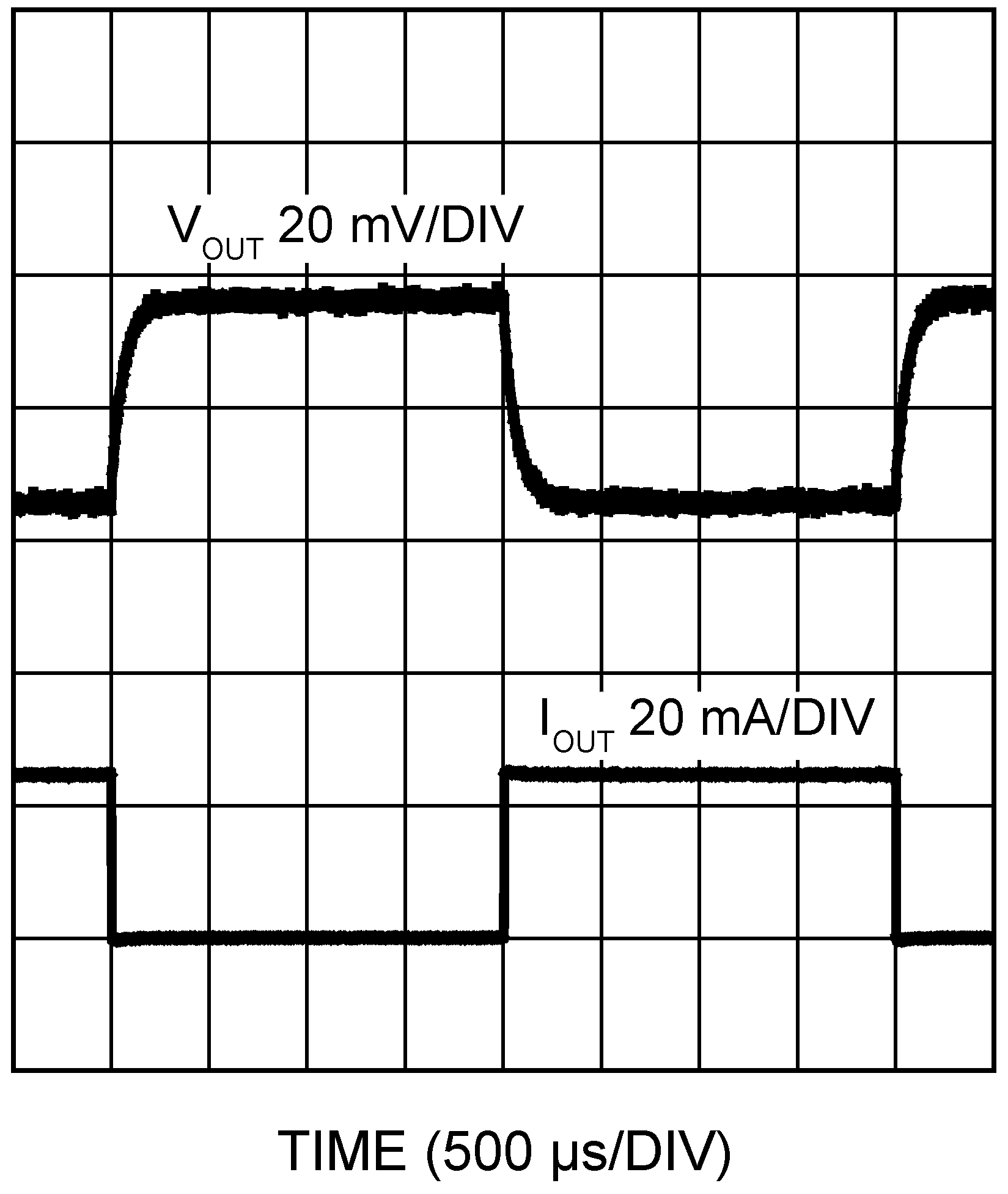 Figure 27. Charge Pump Load Transient Response in 1.5× Mode (0 to 25.5 mA)
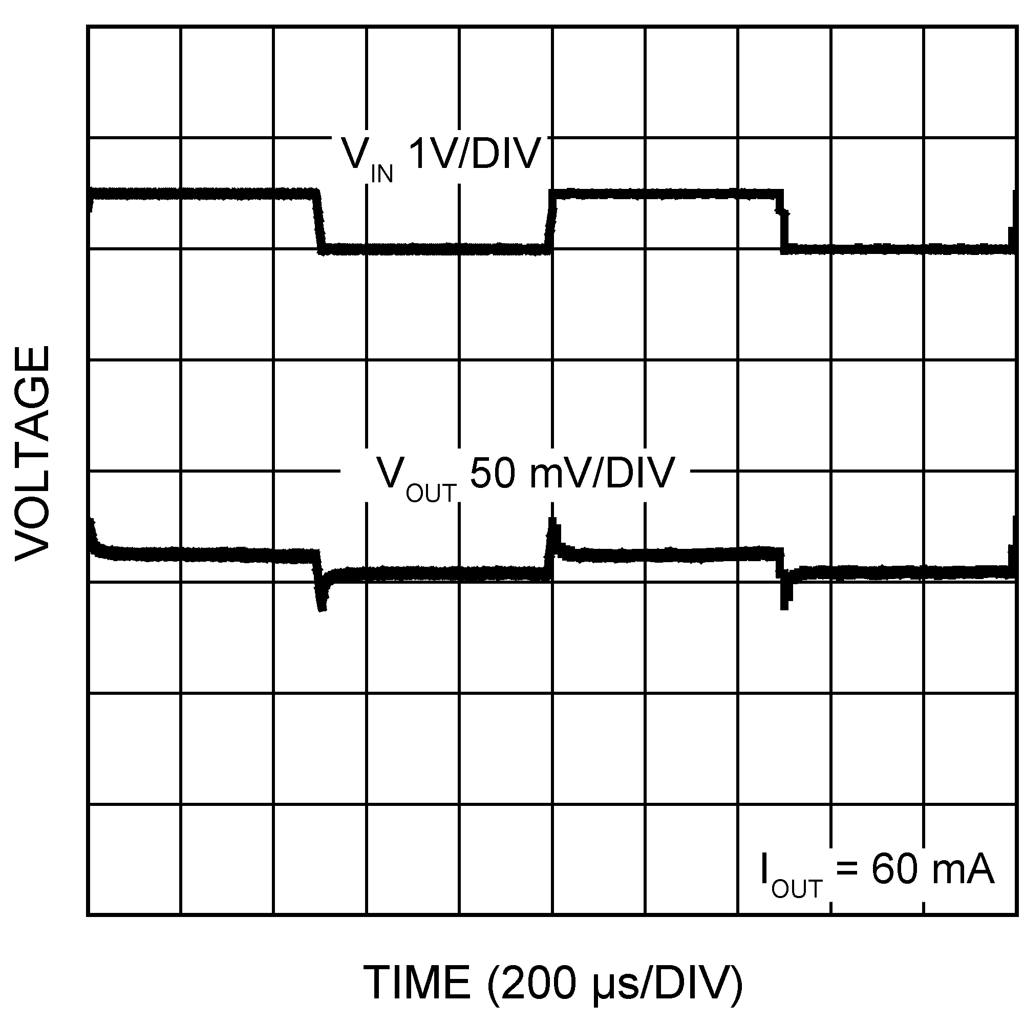 Figure 28. Charge Pump Line Transient Response
1.5× Mode (VIN 3.5V to 4 V)
8.2.2 Application Without Charge Pump
In this application example the input voltage is high enough to drive the LEDs even without charge pump. In that case the charge pump components are omitted, allowing savings on bill-of-material and also board space. Charge pump must be set to 1× mode (bypass) in this case.
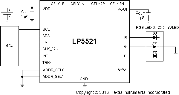 Figure 29. Typical Application Schematic Without Charge Pump
8.2.2.1 Design Requirements
| DESIGN PARAMETER | EXAMPLE VALUE |
|---|---|
| Input voltage range | 4.5 V to 5.5 V |
| LED VF (max) | 3.6 V |
| LED current | 25.5 mA maximum |
| Input capacitor | CIN = 1 μF |
| Output capacitor | COUT = 1 μF |
| Fly capacitors | none |
| Charge pump mode | 1X |
8.2.2.2 Detailed Design Procedures
Selecting input and output capacitors follows the same procedure as in the application with charge pump.
8.3 Initialization Setup
8.3.1 Program Load and Execution Example
-
Startup Device and Configure Device to SRAM Write Mode:
- Supply e.g. 3.6 V to VDD
- Supply e.g. 1.8 V to EN
- Wait 1 ms (startup delay)
- Generate 32 kHz clock to CLK_32K pin
- Write to address 00H 0100 0000b (enable LP5521)
- Wait 500 μs (startup delay)
- Write to address 01H 0001 0000b (Configure R channel into "Load program to SRAM" mode)
-
Program Load to SRAM (see Figure 30):
- Write to address 10H 0000 0011b (1st ramp command 8 MSB)
- Write to address 11H 0111 1111b (1st ramp command 8 LSB)
- Write to address 12H 0100 1101b (1st wait command 8 MSB)
- Write to address 13H 0000 0000b (1st wait command 8 LSB)
- Write to address 14H 0000 0011b (2nd ramp command 8 MSB)
- Write to address 15H 1111 1111b (2nd ramp command 8 LSB)
- Write to address 16H 0110 0000b (2nd wait command 8 MSB)
- Write to address 17H 0000 0000b (2nd wait command 8 LSB)
-
Enable Powersave, charge pump automatic mode (1x / 1.5x) and use external 32 kHz clock:
- Write to address 08H 0011 1000b
-
Run program:
- Write to address 01H 0010 0000b (Configure LED controller operation mode to "Run program" in R channel
- Write to address 00H 0110 0000b (Configure program execution mode from "Hold" to "Run" in R channel
LP5521 will generate 1100 ms long LED pattern which will be repeated infinitely. LED pattern is illustrated in Figure 30.
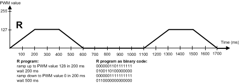 Figure 30. Sequence Diagram
8.3.2 Direct PWM Control Example
-
Start up device:
- Supply, for example, 3.6 V to VDD
- Supply, for example,1.8 V to EN
- Wait 1 ms (start-up delay)
- Write to address 00H 0100 0000b (enable LP5521)
- Wait 500 µs (start-up delay)
-
Enable charge pump 1.5x mode and use internal clock:
- Write to address 08H 0001 0001b
-
Direct PWM control:
- Write to address 01H 0011 1111b (Configure R, G and B channels into "Direct PWM control mode")
-
Write PWM values:
- Write to address 02H 1000 0000b (R driver PWM 50% duty cycle)
- Write to address 03H 1100 0000b (G driver PWM 75% duty cycle)
- Write to address 04H 1111 1111b (B driver PWM 100% duty cycle)
LEDs are turned on after the PWM values are written. Changes to the PWM value registers are reflected immediately to the LED brightness. Default LED current (17.5 mA) is used for LED outputs, if no other values are written.