SNVS441I January 2007 – November 2016 LP5521
PRODUCTION DATA.
- 1 Features
- 2 Applications
- 3 Description
- 4 Revision History
- 5 Pin Configuration and Functions
-
6 Specifications
- 6.1 Absolute Maximum Ratings
- 6.2 ESD Ratings
- 6.3 Recommended Operating Conditions
- 6.4 Thermal Information
- 6.5 Electrical Characteristics
- 6.6 Charge Pump Electrical Characteristics
- 6.7 LED Driver Electrical Characteristics (R, G, B Outputs)
- 6.8 Logic Interface Characteristics
- 6.9 I2C Timing Requirements (SDA, SCL)
- 6.10 Typical Characteristics
-
7 Detailed Description
- 7.1 Overview
- 7.2 Functional Block Diagram
- 7.3 Feature Description
- 7.4 Device Functional Modes
- 7.5 Programming
- 7.6
Register Maps
- 7.6.1 Enable Register (Enable)
- 7.6.2 Operation Mode Register (OP Mode)
- 7.6.3 R Channel PWM Control (R_PWM)
- 7.6.4 G Channel PWM Control (G_PWM)
- 7.6.5 B Channel PWM Control (B_PWM)
- 7.6.6 R Channel Current (R_CURRENT)
- 7.6.7 G Channel Current (G_CURRENT)
- 7.6.8 B Channel Current (B_CURRENT)
- 7.6.9 Configuration Control (CONFIG)
- 7.6.10 R Channel Program Counter Value (R Channel PC)
- 7.6.11 G Channel Program Counter Value (G Channel PC)
- 7.6.12 B Channel Program Counter Value (B Channel PC)
- 7.6.13 Status/Interrupt Register
- 7.6.14 RESET Register
- 7.6.15 GPO Register
- 7.6.16 Program Memory
- 8 Application and Implementation
- 9 Power Supply Recommendations
- 10Layout
- 11Device and Documentation Support
- 12Mechanical, Packaging, and Orderable Information
Package Options
Mechanical Data (Package|Pins)
Thermal pad, mechanical data (Package|Pins)
Orderable Information
7 Detailed Description
7.1 Overview
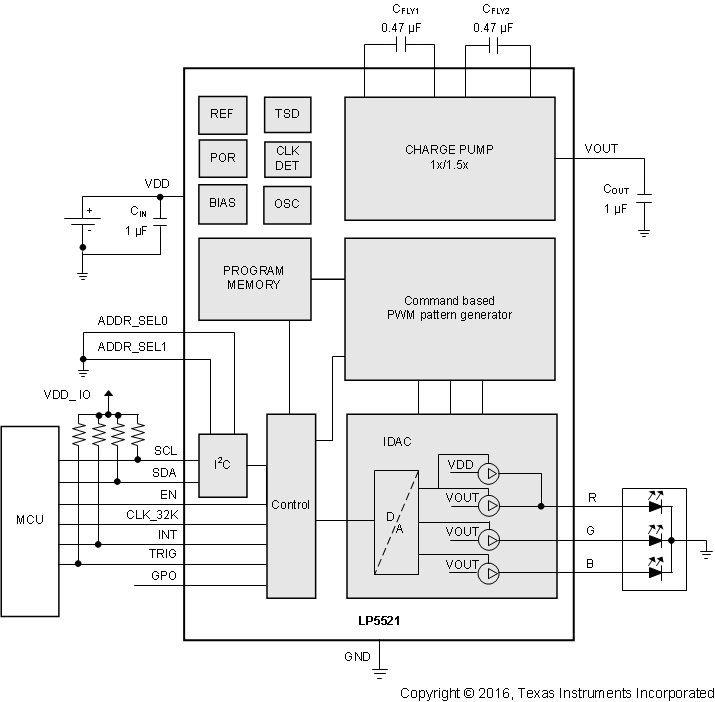
The LP5521 is a three-channel LED driver designed to produce variety of lighting effects for mobile devices. A high-efficiency charge pump enables LED driving over full Li-Ion battery voltage range. The device has a program memory for creating variety of lighting sequences. When program memory has been loaded, the LP5521 can operate autonomously without processor control allowing power savings.
The device maintains excellent efficiency over a wide operating range by automatically selecting proper charge pump gain based on LED forward voltage requirements. the LP5521 is able to automatically enter power-save mode, when LED outputs are not active and thus lowering current consumption.
Three independent LED channels have accurate programmable current sources and PWM control. Each channel has program memory for creating desired lighting sequences with PWM control.
The LP5521 has a flexible digital interface. A trigger I/O and 32-kHz clock input allow synchronization between multiple devices. Interrupt output can be used to notify processor, when LED sequence has ended. LP5521 has four pin-selectable I2C-compatible addresses. This allows connecting up to four parallel devices in one I2C-compatible bus. GPO and INT pins can be used as a digital control pin for other devices.
The LP5521 requires only four small and low-cost ceramic capacitors.
Comprehensive application tools are available, including command compiler for easy LED sequence programming.
7.2 Functional Block Diagram
7.3 Feature Description
7.3.1 Charge Pump Operational Description
The LP5521 includes a pre-regulated switched-capacitor charge pump with a programmable voltage multiplication of 1 and 1.5×.
In 1.5× mode by combining the principles of a switched-capacitor charge pump and a linear regulator, the device generates a regulated 4.5-V output from Li-Ion input voltage range. A two-phase non-overlapping clock generated internally controls the operation of the charge pump. During the charge phase, both flying capacitors (CFLY1 and CFLY2) are charged from input voltage. In the pump phase that follows, the flying capacitors are discharged to output. A traditional switched capacitor charge pump operating in this manner uses switches with very low on-resistance, ideally 0 Ω, to generate an output voltage that is 1.5× the input voltage. The LP5521 regulates the output voltage by controlling the resistance of the input-connected pass-transistor switches in the charge pump.
7.3.1.1 Output Resistance
At lower input voltages, the charge pump output voltage may degrade due to effective output resistance (ROUT) of the charge pump. The expected voltage drop can be calculated by using a simple model for the charge pump shown in Figure 14.
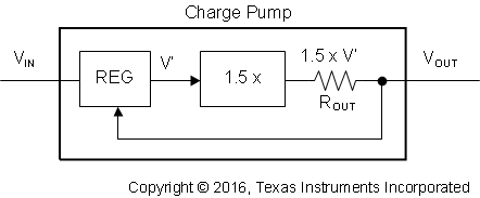 Figure 14. Charge Pump Block Diagram
The model shows a linear pre-regulation block (REG), a voltage multiplier (1.5×), and an output resistance (ROUT). Output resistance models the output voltage drop that is inherent to switched capacitor converters. The output resistance is 3.5 Ω (typical) and is function of switching frequency, input voltage, capacitance value of the flying capacitors, internal resistances of switches, and ESR of flying capacitors. When the output voltage is in regulation, the regulator in the model controls the voltage V’ to keep the output voltage equal to 4.5 V (typical). With increased output current, the voltage drop across ROUT increases. To prevent drop in output voltage, the voltage drop across the regulator is reduced, V’ increases, and VOUT remains at 4.5 V. When the output current increases to the point that there is zero voltage drop across the regulator, V’ equals the input voltage, and the output voltage is on the edge of regulation. Additional output current causes the output voltage to fall out of regulation, so that the operation is similar to a basic open-loop 1.5× charge pump. In this mode, output current results in output voltage drop proportional to the output resistance of the charge pump. The out-of-regulation output voltage can be approximated by: VOUT= 1.5 × VIN – IOUT × ROUT.
7.3.1.2 Controlling Charge Pump
The charge pump is controlled with two CP_MODE bits in register 08H. When both bits are low, the charge pump is disabled, and the output voltage is pulled down with 300 kΩ. Charge pump can be forced to bypass mode, so that battery voltage is going directly to RGB outputs. In 1.5× mode output voltage is boosted to 4.5 V. In automatic mode, charge pump operation mode is defined by LED outputs saturation described in LED Forward Voltage Monitoring. Table 1 lists operation modes and selection bits.
Table 1. CONFIG Register (08H)
| NAME | BIT | DESCRIPTION |
|---|---|---|
| CP_MODE | 4:3 | Charge pump operation mode 00b = OFF 01b = Forced to bypass mode (1×) 10b = Forced to 1.5× mode 11b = Automatic mode selection |
7.3.1.3 LED Forward Voltage Monitoring
When charge pump automatic mode selection is enabled, voltages over LED drivers are monitored. If drivers do not have enough headroom, charge pump gain is set to 1.5×. Driver saturation monitor does not have a fixed voltage limit, since saturation voltage is a function of temperature and current. Charge pump gain is set to 1×, when battery voltage is high enough to supply all LEDs.
In automatic gain change mode, charge pump is switched to bypass mode (1×), when LEDs are inactive for over 50 ms.
Charge pump gain control utilizes digital filtering to prevent supply voltage disturbances from triggering gain changes. If the R driver current source is connected to a battery (address 08H, bit R_TO_BATT = 1), voltage monitoring is disabled in R output, but still functional in B and G outputs.
LED forward voltage monitoring and gain control block diagram is shown in Figure 15.
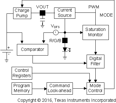 Figure 15. Voltage Monitoring Block Diagram for One Output
7.3.2 LED Driver Operational Description
The LP5521 LED drivers are constant current sources with 8-bit PWM control. Output current can be programmed with I2C register up to 25.5 mA. Current setting resolution is 100 μA (8-bit control).
R driver has two modes: current source can be connected to the battery (VDD) or to the charge pump output. If a current source is connected to the battery, automatic charge pump gain control is not used for this output. This approach provides better efficiency when LED with low VF is connected to R driver, and battery voltage is high enough to drive this LED in all conditions. R driver mode can be selected with I2C register bit. When address 08H, bit R_TO_BATT = 1, R current source is connected to battery. When it is 0 (default), R current source is connected to charge pump same way as in G and B drivers. G and B drivers are always connected to charge pump output.
Some LED configuration examples are given in Table 2. When LEDs with low VF are used, charge pump can be operating in bypass mode (1×). This eliminates the need of having double drivers for all outputs; one connected to battery and another connected to charge pump output. When LP5521 is driving a RGB LED, R channel can be configured to use battery power. This configuration increases power efficiency by minimizing the voltage drop across the LED driver.
Table 2. LED Configuration Examples
| CONFIGURATION | R OUTPUT TO BATT | R OUTPUT TO CP | CP MODE |
|---|---|---|---|
| RGB LED with low VF red | X | Auto (1× or 1.5×) | |
| 3 × low VF LED | X | 1× | |
| 3 × white LED | X | Auto (1× or 1.5×) | |
| 1 × low VF LED (R output) | X | Disabled |
PWM frequency is either 256 Hz or 558 Hz, frequency is set with PWM_HF bit in register 08H. When PWM_HF is 0, the frequency is 256 Hz, and when bit is 1, the PWM frequency is 558 Hz. Brightness adjustment is either linear or logarithmic. This can be set with register 00H LOG_EN bit. When LOG_EN = 0 linear adjustment scale is used, and when LOG_EN = 1 logarithmic scale is used. By using logarithmic scale the visual effect seems linear to the eye. Register control bits are presented in Table 3, Table 4, and Table 5:
Table 3. R_CURRENT Register (05H), G_CURRENT register (06H), B_CURRENT register (07H):
| NAME | BIT | DESCRIPTION | |||
|---|---|---|---|---|---|
| CURRENT | 7:0 | Current setting | |||
| bin | hex | dec | mA | ||
| 0000 0000 0000 0001 0000 0010 0000 0011 0000 0100 0000 0101 0000 0110 ... 1010 1111 ... 1111 1011 1111 1100 1111 1101 1111 1110 1111 1111 |
00 01 02 03 04 05 06 ... AF ... FB FC FD FE FF |
0 1 2 3 4 5 6 ... 175 ... 251 252 253 254 255 |
0.0 0.1 0.2 0.3 0.4 0.5 0.6 ... 17.5 (def) ... 25.1 25.2 25.3 25.4 25.5 |
||
Table 4. ENABLE Register (00H):
| NAME | BIT | DESCRIPTION |
|---|---|---|
| LOG_EN | 7 | Logarithmic PWM adjustment enable bit 0 = Linear adjustment 1 = Logarithmic adjustment |
Table 5. CONFIG Register (08H):
| NAME | BIT | DESCRIPTION |
|---|---|---|
| PWM_HF | 6 | PWM clock frequency 0 = 256 Hz, frequency defined by the 32-kHz clock (internal or external) 1 = 558 Hz, frequency defined by internal oscillator |
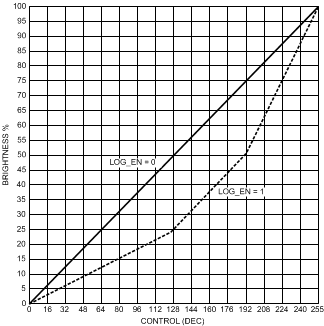 Figure 16. Logarithmic and Linear PWM Adjustment Curves
7.3.3 Automatic Power Save
Automatic power save mode is enabled when PWRSAVE_EN bit in register address 08H is 1. Almost all analog blocks are powered down in power save, if external clock is used. Only charge pump protection circuits remain active. However if internal clock has been selected only charge pump and led drivers are disabled during power save since digital part of the LED controller need to remain active. In both cases charge pump enters 'weak 1×' mode. In this mode charge pump utilizes a passive current limited keep-alive switch, which keeps the output voltage at battery level.
During program execution LP5521 can enter power save if there is no PWM activity in R, G and B outputs. To prevent short power save sequences during program execution, LP5521 has command look-ahead filter. In every instruction cycle R, G, B commands are analyzed, and if there is sufficient time left with no PWM activity, the device enters power save. In power save program execution continues uninterruptedly. When a command that requires PWM activity is executed, fast internal start-up sequence will be started automatically. Table 6 describe commands and conditions that can activate power save. All channels (R,G,B) need to meet power save condition in order to enable power save.
Table 6. LED Controller Operation
| LED CONTROLLER OPERATION
MODE (R,G,B_MODE) |
POWER SAVE CONDITION |
|---|---|
| 00b | Disabled mode enables power save |
| 01b | Load program to SRAM mode prevents power save |
| 10b | Run program mode enables power save if there is no PWM activity and command look-ahead filter condition is met |
| 11b | Direct control mode enables power save if there is no PWM activity |
| COMMAND | POWER SAVE CONDITION |
|---|---|
| Wait | No PWM activity and current command wait time longer than 50 ms. If prescale = 1 then wait time needs to be longer than 80 ms. |
| Ramp | Ramp Command PWM value reaches minimum 0 and current command execution time left more than 50 ms. If prescale = 1 then time left needs to be more than 80 ms. |
| Trigger | No PWM activity during wait for trigger command execution. |
| End | No PWM activity or Reset bit = 1 |
| Set PWM | Enables power save if PWM set to 0 and next command generates at least 50 ms wait |
| Other commands | No effect to power save |
See application note LP5521 Power Efficiency Considerations (SNVA185) for more information.
7.3.4 External Clock Detection
The presence of external clock can be detected by the LP5521. Program execution is clocked with internal 32 kHz clock or with external clock. Clocking is controlled with register address 08H bits, INT_CLK_EN and CLK_DET_EN as seen on the following table.
External clock can be used if clock is present at CLK_32K pin. External clock frequency must be 32 kHz for the program execution / PWM timing to be like specified. If higher or lower frequency is used, it will affect the program engine execution speed. If other than 32 kHz clock frequency is used, the program execution timings must be scaled accordingly. The external clock detector block only detects too low clock frequency (< 15 kHz). If external clock frequency is higher than specified, the external clock detector notifies that external clock is present. External clock status can be checked with read only bit EXT_CLK_USED in register address 0CH, when the external clock detection is enabled (CLK_DET_EN bit = high). If EXT_CLK_USED = 1, then the external clock is detected and it is used for timing, if automatic clock selection is enabled (see Table 7).
If external clock is stuck-at-zero or stuck-at-one, or the clock frequency is too low, the clock detector indicates that external clock is not present.
If external clock is not used on the application, connect the CLK_32K pin to GND to prevent floating of this pin and extra current consumption.
Table 7. CONFIG Register (08H):
| NAME | BIT | DESCRIPTION |
|---|---|---|
| CLK_DET_EN, INT_CLK_EN |
1:0 | LED controller clock source 00b = External clock source (CLK_32K) 01b = Internal clock 10b = Automatic selection 11b = Internal clock |
7.3.5 Logic Interface Operational Description
LP5521 features a flexible logic interface for connecting to processor and peripheral devices. Communication is done with I2C compatible interface and different logic input/output pins makes it possible to synchronize operation of several devices.
7.3.5.1 I/O Levels
I2C interface, CLK_32K and TRIG pins input levels are defined by EN pin. Using EN pin as voltage reference for logic inputs simplifies PWB routing and eliminates the need for dedicated VIO pin. Figure 17 describes EN pin connections.
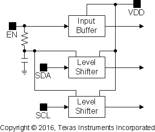 Figure 17. Using EN Pin as Digital I/O Voltage Reference
ADDR_SEL0/1 are referenced to VDD voltage. GPO pin level is defined by VDD voltage.
7.3.5.2 GPO/INT Pins
LP5521 has one General Purpose Output pin (GPO); the INT pin can also be configured as a GPO pin. When INT is configured as GPO output, its level is defined by the VDD voltage. State of the pins can be controlled with GPO register (0EH). GPO pins are digital CMOS outputs and no pullup or pulldown resistors are needed.
When INT pin GPO function is disabled, it operates as an open drain pin. INT signal is active low; that is, when interrupt signal is sent, the pin is pulled to GND. External pullup resistor is needed for proper functionality.
Table 8. GPO Register (0EH)
| NAME | BIT | DESCRIPTION |
|---|---|---|
| INT_AS_GPO | 2 | Enable INT pin GPO function 0 = INT pin functions as a INT pin 1 = INT pin functions as a GPO pin |
| GPO | 1 | 0 = GPO pin state is low 1 = GPO pin state is high |
| INT | 0 | 0 = INT pin state is low (INT_AS_GPO=1) 1 = INT pin state is high (INT_AS_GPO=1) |
7.3.5.3 TRIG Pin
The TRIG pin can function as an external trigger input or output. External trigger signal is active low; that is, when trigger is sent or received the pin is pulled to GND. TRIG is an open-drain pin and external pullup resistor is needed for trigger line. External trigger input signal must be at least two 32-kHz clock cycles long to be recognized. Trigger output signal is three 32-kHz clock cycles long. If TRIG pin is not used on application, connected the TRIG pin to GND to prevent floating of this pin and extra current consumption.
7.3.5.4 ADDR_SEL0,1 Pins
The ADDR_SEL0,1 pins define the chip I2C address. Pins are referenced to VDD signal level. See I2C-Compatible Serial Bus Interface for I2C address definitions.
7.3.5.5 CLK_32K Pin
The CLK_32K pin is used for connecting an external 32-kHz clock to LP5521. External clock can be used to synchronize the sequence engines of several LP5521. Using external clock can also improve automatic power save mode efficiency, because internal clock can be switched off automatically when device has entered power save mode, and external clock is present. See application note LP5521 Power Efficiency Considerations (SNVA185) for more information.
Device can be used without the external clock. If external clock is not used on the application, connect the CLK_32K pin to GND to prevent floating of this pin and extra current consumption.
7.4 Device Functional Modes
7.4.1 Modes of Operation
-
RESET:In the RESET mode all the internal registers are reset to the default values. Reset is done always if Reset Register (0DH) is written FFH or internal power on reset (POR) is activated. POR activates when supply voltage is connected or when the supply voltage VDD falls below 1.5 V typical (0.8 V minimum). Once VDD rises above 1.5 V, POR inactivates, and the chip continues to the STANDBY mode. CHIP_EN control bit is low after POR by default.
-
STANDBY:The STANDBY mode is entered if the register bit CHIP_EN or EN pin is LOW and Reset is not active. This is the low power consumption mode, when all circuit functions are disabled. Registers can be written in this mode if EN pin is high. Control bits are effective after start-up.
-
START-UP:When CHIP_EN bit is written high and EN pin is high, the INTERNAL STARTUP SEQUENCE powers up all the needed internal blocks (VREF, bias, oscillator, etc.). Start-up delay is after setting EN pin high is 1 ms (typical). Start-up delay after setting CHIP_EN to 1 is 500 μs (typical). If the chip temperature rises too high, the thermal shutdown (TSD) disables the chip operation, and the chip state is in START-UP mode until no TSD event is present.(4)
-
NORMAL:During NORMAL mode the user controls the chip using the Control Registers. If EN pin is set low, the CHIP_EN bit is reset to 0.
-
POWER SAVE:In POWER SAVE mode analog blocks are disabled to minimize power consumption. See Automatic Power Save for further information.
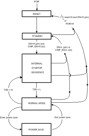 Figure 18. Modes of Operation
7.5 Programming
7.5.1 I2C-Compatible Serial Bus Interface
7.5.1.1 Interface Bus Overview
The I2C compatible synchronous serial interface provides access to the programmable functions and registers on the device. This protocol uses a two-wire interface for bidirectional communications between the IC's connected to the bus. The two interface lines are the serial data line (SDA), and the serial clock line (SCL). These lines should be connected to a positive supply, via a pullup resistor and remain HIGH even when the bus is idle.
Every device on the bus is assigned a unique address and acts as either a Master or a Slave depending on whether it generates or receives the serial clock (SCL).
7.5.1.2 Data Transactions
One data bit is transferred during each clock pulse. Data is sampled during the high state of the serial clock (SCL). Consequently, throughout the high period of the clock the data should remain stable. Any changes on the SDA line during the high state of the SCL and in the middle of a transaction, aborts the current transaction. New data should be sent during the low SCL state. This protocol permits a single data line to transfer both command/control information and data using the synchronous serial clock.
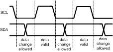 Figure 19. Data Validity
Each data transaction is composed of a start condition, a number of byte transfers (set by the software) and a stop condition to terminate the transaction. Every byte written to the SDA bus must be 8 bits long and is transferred with the most significant bit first. After each byte, an acknowledge signal must follow. The following sections provide further details of this process.
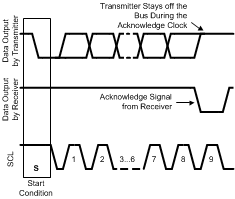 Figure 20. Acknowledge Signal
The Master device on the bus always generates the start and stop conditions (control codes). After a start condition is generated, the bus is considered busy and it retains this status until a certain time after a stop condition is generated. A high-to-low transition of the data line (SDA) while the clock (SCL) is high indicates a start condition. A low-to-high transition of the SDA line while the SCL is high indicates a stop condition.
 Figure 21. Start and Stop Conditions
In addition to the first start condition, a repeated start condition can be generated in the middle of a transaction. This allows another device to be accessed, or a register read cycle.
7.5.1.3 Acknowledge Cycle
The acknowledge cycle consists of two signals: the acknowledge clock pulse the master sends with each byte transferred, and the acknowledge signal sent by the receiving device.
The master generates the acknowledge clock pulse on the ninth clock pulse of the byte transfer. The transmitter releases the SDA line (permits it to go high) to allow the receiver to send the acknowledge signal. The receiver must pull down the SDA line during the acknowledge clock pulse and ensure that SDA remains low during the high period of the clock pulse, thus signaling the correct reception of the last data byte and its readiness to receive the next byte.
7.5.1.4 Acknowledge After Every Byte Rule
The master generates an acknowledge clock pulse after each byte transfer. The receiver sends an acknowledge signal after every byte received.
There is one exception to the acknowledge after every byte rule. When the master is the receiver, it must indicate to the transmitter an end of data by not-acknowledging (negative acknowledge) the last byte clocked out of the slave. This negative acknowledge still includes the acknowledge clock pulse (generated by the master), but the SDA line is not pulled down.
7.5.1.5 Addressing Transfer Formats
Each device on the bus has a unique slave address. The LP5521 operates as a slave device with the 7-bit address. The LP5521 I2C address is pin selectable from four different choices. If 8-bit address is used for programming, the 8th bit is 1 for read and 0 for write. Table 9 shows the 8-bit I2C addresses.
Table 9. 8-Bit I2C Addresses
| ADDR_SEL [1:0] |
I2C ADDRESS WRITE (8 bits) |
I2C ADDRESS READ (8 bits) |
|---|---|---|
| 00 01 10 11 |
0110 0100 = 64H 0110 0110 = 66H 0110 1000 = 68H 0110 1010 = 6AH |
0110 0101 = 65H 0110 0111 = 67H 0110 1001 = 69H 0110 1011 = 6BH |
Before any data is transmitted, the master transmits the address of the slave being addressed. The slave device sends an acknowledge signal on the SDA line, once it recognizes its address.
The slave address is the first seven bits after a start condition. The direction of the data transfer (R/W) depends on the bit sent after the slave address — the eighth bit.
When the slave address is sent, each device in the system compares this slave address with its own. If there is a match, the device considers itself addressed and sends an acknowledge signal. Depending upon the state of the R/W bit (1:read, 0:write), the device acts as a transmitter or a receiver.
 Figure 22. I2C Chip Address
7.5.1.6 Control Register Write Cycle
- Master device generates start condition.
- Master device sends slave address (7 bits) and the data direction bit (r/w = 0).
- Slave device sends acknowledge signal if the slave address is correct.
- Master sends control register address (8 bits).
- Slave sends acknowledge signal.
- Master sends data byte to be written to the addressed register.
- Slave sends acknowledge signal.
- If master will send further data bytes the control register address is incremented by one after acknowledge signal.
- Write cycle ends when the master creates stop condition.
7.5.1.7 Control Register Read Cycle
- Master device generates a start condition.
- Master device sends slave address (7 bits) and the data direction bit (r/w = 0).
- Slave device sends acknowledge signal if the slave address is correct.
- Master sends control register address (8 bits).
- Slave sends acknowledge signal.
- Master device generates repeated start condition.
- Master sends the slave address (7 bits) and the data direction bit (r/w = 1).
- Slave sends acknowledge signal if the slave address is correct.
- Slave sends data byte from addressed register.
- If the master device sends acknowledge signal, the control register address is incremented by one. Slave device sends data byte from addressed register.
- Read cycle ends when the master does not generate acknowledge signal after data byte and generates stop condition.
| ADDRESS MODE | |
|---|---|
| Data Read | <Start Condition> <Slave Address><r/w = 0>[Ack] <Register Addr.>[Ack] <Repeated Start Condition> <Slave Address><r/w = 1>[Ack] [Register Data]<Ack or NAck> … additional reads from subsequent register address possible <Stop Condition> |
| Data Write | <Start Condition> <Slave Address><r/w=’0’>[Ack] <Register Addr.>[Ack] <Register Data>[Ack] … additional writes to subsequent register address possible <Stop Condition> |
<>Data from master [ ] Data from slave
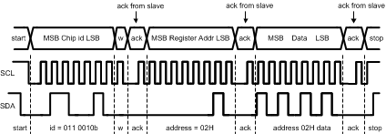 Figure 23. Register Write Format
When a READ function is to be accomplished, a WRITE function must precede the READ function, as shown in Figure 24.

r = read (SDA = 1)
ack = acknowledge (SDA pulled down by either master or slave
rs = repeated start
id = 7-bit chip address
7.5.2 LED Controller Operation Modes
Operation modes are defined in register address 01H. Each output channel (R, G, B) operation mode can be configured separately. MODE registers are synchronized to a 32-kHz clock. Delay between consecutive I2C writes to OP_MODE register (01H) need to be longer than 153 µs (typical).
Table 10. OP_MODE Register (01H):
| NAME | BIT | DESCRIPTION |
|---|---|---|
| R_MODE | 5:4 | R channel operation mode 00b = Disabled, reset R channel PC 01b = Load program to SRAM, reset R channel PC 10b = Run program defined by R_EXEC 11b = Direct control, reset R channel PC |
| G_MODE | 3:2 | G channel operation mode 00b = Disabled, reset G channel PC 01b = Load program to SRAM, reset G channel PC 10b = Run program defined by G_EXEC 11b = Direct control, reset G channel PC |
| B_MODE | 1:0 | B channel operation mode 00b = Disabled, reset B channel PC 01b = Load program to SRAM, reset B channel PC 10b = Run program defined by B_EXEC 11b = Direct control, reset B channel PC |
7.5.2.1 Disabled
Each channel can be configured to disabled mode. LED output current is 0 during this mode. Disabled mode resets PC of respective channel.
7.5.2.2 LOAD Program
LP5521 can store 16 commands for each channel (R, G, B). Each command consists of 16 bits. Because one register has only 8 bits, one command requires two I2C register addresses. In order to reduce program load time LP5521 supports address auto incrementation. Register address is incremented after each 8 data bits. Whole program memory can be written in one I2C write sequence.
Program memory is defined in the LP5521 register table, 10H to 2FH for R channel, 30H to 4FH for G channel and 50H to 6FH for B channel. In order to be able to access program memory at least one channel operation mode needs to be LOAD Program.
Memory writes are allowed only to the channel in LOAD mode. All channels are in hold while one or several channels are in LOAD program mode, and PWM values are frozen for the channels which are not in LOAD mode. Program execution continues when all channels are out of LOAD program mode. LOAD Program mode resets PC of respective channel.
7.5.2.3 RUN Program
RUN Program mode executes the commands defined in program memory for respective channel (R, G, B). Execution register bits in ENABLE register define how program is executed. Program start position can be programmed to Program Counter register (see the following tables). By manually selecting the PC start value, user can write different lighting sequences to the memory, and select appropriate sequence with the PC register. If program counter runs to end (15) the next command will be executed from program location 0.
If internal clock is used in the RUN program mode, operation mode needs to be written disabled (00b) before disabling the chip (with CHIP_EN bit or EN pin) to ensure that the sequence starts from the correct program counter (PC) value when restarting the sequence.
PC registers are synchronized to 32 kHz clock. Delay between consecutive I2C writes to PC registers (09H, 0AH, 0BH) need to be longer than 153 µs (typ.).
Note that entering LOAD program or Direct Control Mode from RUN PROGRAM mode is not allowed. Engine execution mode should be set to Hold, and Operation Mode to disabled, when changing operation mode from RUN mode.
Table 11. R Channel PC Register (09H), G CHANNEL PC Register (0AH), B CHANNEL PC Register (0BH)
| NAME | BIT | DESCRIPTION |
|---|---|---|
| PC | 3:0 | Program counter value from 0 to 15d |
Table 12. ENABLE Register (00H)
| NAME | BIT | DESCRIPTION |
|---|---|---|
| R_EXEC | 5:4 | R channel program execution 00b = Hold: Wait until current command is finished then stop while EXEC mode is hold. PC can be read or written only in this mode. 01b = Step: Execute instruction defined by current R channel PC value, increment PC and change R_EXEC to 00b (Hold) 10b = Run: Start at program counter value defined by current R channel PC value 11b = Execute instruction defined by current R channel PC value and change R_EXEC to 00b (Hold) |
| G_EXEC | 3:2 | G channel program execution 00b = Hold: Wait until current command is finished then stop while EXEC mode is hold. PC can be read or written only in this mode. 01b = Step: Execute instruction defined by current G channel PC value, increment PC and change G_EXEC to 00b (Hold) 10b = Run: Start at program counter value defined by current G channel PC value 11b = Execute instruction defined by current G channel PC value and change G_EXEC to 00b (Hold) |
| B_EXEC | 1:0 | B channel program execution 00b = Hold: Wait until current command is finished then stop while EXEC mode is hold. PC can be read or written only in this mode. 01b = Step: Execute instruction defined by current B channel PC value, increment PC and change B_EXEC to 00b (Hold) 10b = Run: Start at program counter value defined by current B channel PC value 11b = Execute instruction defined by current B channel PC value and change B_EXEC to 00b (Hold) |
EXEC registers are synchronized to 32-kHz clock. Delay between consecutive I2C writes to ENABLE register (00H) need to be longer than 488 μs (typ.).
7.5.2.3.1 DIRECT Control
When R, G or B channel mode is set to 11b, the LP5521 drivers work in direct control mode. LP5521 LED channels can be controlled independently through I2C. For each channel there is a PWM control register and a output current control register. With output current control register is set what is the maximum output current with 8-bit resolution, step size is 100 μA. Duty cycle can be set with 8-bit resolution. Direct control mode resets respective channel’s PC. PWM control bits are presented in Table 13:
Table 13. R_PWM Register (02H), G_PWM Register (03H), B_PWM Register (04H):
| NAME | BIT | DESCRIPTION |
|---|---|---|
| PWM | 7:0 | LED PWM value during direct control operation mode 0000 0000b = 0% 1111 1111b = 100% |
If charge pump automatic gain change is used in this mode, then PWM values need to be written 0 before changing the drivers’ operation mode to disabled (00b) to ensure proper automatic gain change operation.
7.5.3 LED Controller Programming Commands
LP5521 has three independent programmable channels (R, G, B). Trigger connections between channels are common for all channels. All channels have own program memories for storing complex patterns. Brightness control and patterns are done with 8-bit PWM control (256 steps) to get accurate and smooth color control.
Program execution is timed with 32 768 Hz clock. This clock can be generated internally or external 32 kHz clock can be connected to CLK_32K pin. Using external clock enables synchronization of LED timing to this clock rather than internal clock. Selection of the clock is made with address 08H bits INT_CLK_EN and CLK_DET_EN. See External Clock Detection for details.
Supported commands are listed in Table 14. Command compiler is available for easy sequence programming. With Command compiler it is possible to write sequences with simple ASCII commands, which are then converted to binary or hex format. See application note "LP5521 Programming Considerations" for examples of Command compiler usage.
Table 14. LED Controller Programming Commands
| Command | 15 | 14 | 13 | 12 | 11 | 10 | 9 | 8 | 7 | 6 | 5 | 4 | 3 | 2 | 1 | 0 |
|---|---|---|---|---|---|---|---|---|---|---|---|---|---|---|---|---|
| Ramp
Wait |
0 | Pre- scale |
Step time | Sign | Increment (number of steps) | |||||||||||
| Set PWM | 0 | 1 | 0 | PWM Value | ||||||||||||
| Go to Start | 0 | 0 | 0 | 0 | 0 | 0 | 0 | 0 | 0 | 0 | 0 | |||||
| Branch | 1 | 0 | 1 | Loop count | x | Step / command number | ||||||||||
| End | 1 | 1 | 0 | Int | Reset | X | ||||||||||
| Trigger | 1 | 1 | 1 | Wait for trigger on channels 5-0 | Send trigger on channels 5-0 | X | ||||||||||
X means do not care whether 1 or 0.
7.5.3.1 RAMP/WAIT
Ramp command generates a PWM ramp starting from current value. At each ramp step the output is incremented by one. Time for one step is defined with Prescale and Step time bits. Minimum time for one step is 0.49 ms and maximum time is 63 × 15.6 ms = 1 second/step, so it is possible to program very fast and also very slow ramps. Increment value defines how many steps are taken in one command. Number of actual steps is Increment + 1. Maximum value is 127d, which corresponds to half of full scale (128 steps). If during ramp command PWM reaches minimum/maximum (0/255) ramp command is executed to the end, and PWM stays at minimum/maximum. This enables ramp command to be used as combined ramp and wait command in a single instruction.
Ramp command can be used as wait instruction when increment is zero.
Setting register 00H bit LOG_EN sets the scale from linear to logarithmic. When LOG_EN = 0 linear scale is used, and when LOG_EN = 1 logarithmic scale is used. By using logarithmic scale the visual effect of the ramp command seems linear to the eye.
Table 15. Ramp/Wait Command
| 15 | 14 | 13 | 12 | 11 | 10 | 9 | 8 | 7 | 6 | 5 | 4 | 3 | 2 | 1 | 0 |
|---|---|---|---|---|---|---|---|---|---|---|---|---|---|---|---|
| 0 | Pre- scale | Step time | Sign | Increment | |||||||||||
| NAME | VALUE(d) | DESCRIPTION |
|---|---|---|
| Prescale | 0 | Divides master clock (32 768Hz) by 16 = 2048 Hz, 0.49 ms cycle time |
| 1 | Divides master clock (32 768Hz) by 512 = 64 Hz, 15.6 ms cycle time | |
| Step time | 1-63 | One ramp increment done in (step time) x (clock after prescale) Note: 0 means Set PMW command. |
| Sign | 0 | Increase PWM output |
| 1 | Decrease PWM output | |
| Increment | 0-127 | The number of steps is Increment + 1. Note: 0 is a wait instruction. |
Application example:
For example if following parameters are used for ramp:
- Prescale = 1 → cycle time = 15.6 ms
- Step time = 2 → time = 15.6 ms x 2 = 31.2 ms
- Sign = 0 → rising ramp
- Increment = 4 → 5 cycles
Ramp command will be: 0100 0010 0000 0100b = 4204H
If current PWM value is 3, and the first command is as described above and next command is a ramp with otherwise same parameters, but with Sign = 1 (Command = 4284H), the result will be like in Figure 25:
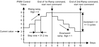 Figure 25. Example of 2 Sequential Ramp Commands.
7.5.3.2 Set PWM
Set PWM output value from 0 to 255. Command takes sixteen 32 kHz clock cycles (= 488 μs). Setting register 00H bit LOG_EN sets the scale from linear to logarithmic.
Table 16. Set PWM Command
| 15 | 14 | 13 | 12 | 11 | 10 | 9 | 8 | 7 | 6 | 5 | 4 | 3 | 2 | 1 | 0 |
|---|---|---|---|---|---|---|---|---|---|---|---|---|---|---|---|
| 0 | 1 | 0 | 0 | 0 | 0 | 0 | 0 | PWM value | |||||||
7.5.3.3 Go to Start
Go to start command resets Program Counter register and continues executing program from the 00H location. Command takes sixteen 32 kHz clock cycles. Note that default value for all program memory registers is 0000H, which is Go to start command.
| Go to start command | |||||||||||||||
|---|---|---|---|---|---|---|---|---|---|---|---|---|---|---|---|
| 15 | 14 | 13 | 12 | 11 | 10 | 9 | 8 | 7 | 6 | 5 | 4 | 3 | 2 | 1 | 0 |
| 0 | 0 | 0 | 0 | 0 | 0 | 0 | 0 | 0 | 0 | 0 | 0 | 0 | 0 | 0 | 0 |
7.5.3.4 Branch
When branch command is executed, the 'step number' value is loaded to PC and program execution continues from this location. Looping is done by the number defined in loop count parameter. Nested looping is supported (loop inside loop). The number of nested loops is not limited. Command takes sixteen 32-kHz clock cycles.
Table 17. Branch Command
| 15 | 14 | 13 | 12 | 11 | 10 | 9 | 8 | 7 | 6 | 5 | 4 | 3 | 2 | 1 | 0 |
|---|---|---|---|---|---|---|---|---|---|---|---|---|---|---|---|
| 1 | 0 | 1 | Loop count | X | X | X | Step number | ||||||||
| NAME | VALUE(d) | DESCRIPTION |
|---|---|---|
| loop count | 0-63 | The number of loops to be done. 0 means infinite loop. |
| step number | 0-15 | The step number to be loaded to program counter. |
7.5.3.5 End
End program execution, resets the program counter and sets the corresponding EXEC register to 00b (hold). Command takes sixteen 32-kHz clock cycles.
Table 18. End Command
| 15 | 14 | 13 | 12 | 11 | 10 | 9 | 8 | 7 | 6 | 5 | 4 | 3 | 2 | 1 | 0 |
|---|---|---|---|---|---|---|---|---|---|---|---|---|---|---|---|
| 1 | 1 | 0 | int | reset | X | X | X | X | X | X | X | X | X | X | X |
| NAME | VALUE | DESCRIPTION |
|---|---|---|
| int | 0 | No interrupt will be sent. |
| 1 | Send interrupt to processor by pulling the INT pin down and setting corresponding status register bit high to notify that program has ended. Interrupt can only be cleared by reading interrupt status register 0CH. | |
| reset | 0 | Keep the current PWM value. |
| 1 | Set PWM value to 0. |
X means do not care whether 1 or 0.
7.5.3.6 Trigger
Wait or send triggers can be used to, for example, synchronize operation between different channels. Send trigger command takes sixteen 32-kHz clock cycles, and wait for trigger takes at least sixteen 32 kHz clock cycles. The receiving channel stores sent triggers. Received triggers are cleared by wait for trigger command if received triggers match to channels defined in the command. Channel waits for until all defined triggers have been received.
External trigger input signal must be at least two 32-kHz clock cycles (= 61 μs typical) long to be recognized. Trigger output signal is three 32-kHz clock cycles (92 μs typical) long. External trigger signal is active low; that is, when trigger is sent/received the pin is pulled to GND. Sent external trigger is masked; that is, the device which has sent the trigger does not recognize it. If send and wait external trigger are used on the same command, the send external trigger is executed first, then the wait external trigger.
Table 19. Trigger Command
| 15 | 14 | 13 | 12 | 11 | 10 | 9 | 8 | 7 | 6 | 5 | 4 | 3 | 2 | 1 | 0 |
|---|---|---|---|---|---|---|---|---|---|---|---|---|---|---|---|
| 1 | 1 | 1 | wait trigger <5:0> | send trigger <5:0> | X | ||||||||||
| EXT | X | B | G | R | EXT | X | B | G | R | ||||||
| NAME | VALUE(d) | DESCRIPTION |
|---|---|---|
| wait trigger<5:0> | 0-31 | Wait for trigger for the channel(s) defined. Several triggers can be defined in the same command. Bit 0 is R, bit 1 is G, bit 2 is B and bit 5 is external trigger I/O. Bits 3 and 4 are not in use. |
| send trigger<5:0> | 0-31 | Send trigger for the channel(s) defined. Several triggers can be defined in the same command. Bit 0 is R, bit 1 is G, bit 2 is B and bit 5 is external trigger I/O. Bits 3 and 4 are not in use. |
X means do not care whether 1 or 0.
7.6 Register Maps
Table 20. LP5521 Control Register Names and Default Values
| ADDR (HEX) | REGISTER | D7 | D6 | D5 | D4 | D3 | D2 | D1 | D0 | DEFAULT |
|---|---|---|---|---|---|---|---|---|---|---|
| 00 | ENABLE | LOG_EN | CHIP_EN | R_EXEC[1:0] | G_EXEC[1:0] | B_EXEC[1:0] | 0000 0000 | |||
| 01 | OP MODE | R_MODE[1:0] | G_MODE[1:0] | B_MODE[1:0] | 0000 0000 | |||||
| 02 | R PWM | R_PWM[7:0] | 0000 0000 | |||||||
| 03 | G PWM | G_PWM[7:0] | 0000 0000 | |||||||
| 04 | B PWM | B_PWM[7:0] | 0000 0000 | |||||||
| 05 | R CURRENT | R_CURRENT[7:0] | 1010 1111 | |||||||
| 06 | G CURRENT | G_CURRENT[7:0] | 1010 1111 | |||||||
| 07 | B CURRENT | B_CURRENT[7:0] | 1010 1111 | |||||||
| 08 | CONFIG | PWM_HF | PWRSAVE_EN | CP_MODE[1:0] | R_TO_BATT | CLK_DET_EN | INT_CLK_EN | 0000 0000 | ||
| 09 | R PC | R_PC[3:0] | 0000 0000 | |||||||
| 0A | G PC | G_PC[3:0] | 0000 0000 | |||||||
| 0B | B PC | B_PC[3:0] | 0000 0000 | |||||||
| 0C | STATUS | EXT_CLK_USED | R_INT | G_INT | B_INT | 0000 0000 | ||||
| 0D | RESET | RESET[7:0] | 0000 0000 | |||||||
| 0E | GPO | INT_AS_GPO | GPO | INT | 0000 0000 | |||||
| 10 | PROG MEM R | CMD_R1[15:8] | 0000 0000 | |||||||
| 11 | PROG MEM R | CMD_R1[7:0] | 0000 0000 | |||||||
| ... | ||||||||||
| 2E | PROG MEM R | CMD_R16[15:8] | 0000 0000 | |||||||
| 2F | PROG MEM R | CMD_R16[7:0] | 0000 0000 | |||||||
| 30 | PROG MEM G | CMD_G1[15:8] | 0000 0000 | |||||||
| 31 | PROG MEM G | CMD_G1[7:0] | 0000 0000 | |||||||
| ... | ||||||||||
| 4E | PROG MEM G | CMD_G16[15:8] | 0000 0000 | |||||||
| 4F | PROG MEM G | CMD_G16[7:0] | 0000 0000 | |||||||
| 50 | PROG MEM B | CMD_B1[15:8] | 0000 0000 | |||||||
| 51 | PROG MEM B | CMD_B1[7:0] | 0000 0000 | |||||||
| ... | ||||||||||
| 6E | PROG MEM B | CMD_B16[15:8] | 0000 0000 | |||||||
| 6F | PROG MEM B | CMD_B16[7:0] | 0000 0000 | |||||||
7.6.1 Enable Register (Enable)
Address 00H
Reset value 00H
Table 21. Enable Register
| 7 | 6 | 5 | 4 | 3 | 2 | 1 | 0 |
|---|---|---|---|---|---|---|---|
| LOG_EN | CHIP_EN | R_EXEC[1] | R_EXEC[0] | G_EXEC[1] | G_EXEC[0] | B_EXEC[1] | B_EXEC[0] |
| NAME | BIT | ACCESS | ACTIVE | DESCRIPTION |
|---|---|---|---|---|
| LOG_EN | 7 | R/W | High | Logarithmic PWM adjustment generation enable |
| CHIP_EN | 6 | R/W | High | Master chip enable. Enables device internal startup sequence. Startup delay after setting CHIP_EN is 500 μs. See Operation for further information. Setting EN pin low resets the CHIP_EN state to 0. |
| R_EXEC | 5:4 | R/W | R channel program execution. 00b = Hold: Wait until current command is finished then stop while EXEC mode is hold. PC can be read or written only in this mode. 01b = Step: Execute instruction defined by current R channel PC value, increment PC and change R_EXEC to 00b (Hold) 10b = Run: Start at program counter value defined by current R Channel PC value 11b = Execute instruction defined by current R channel PC value and change R_EXEC to 00b (Hold) |
|
| G_EXEC | 3:2 | R/W | G channel program execution 00b = Hold: Wait until current command is finished then stop while EXEC mode is hold. PC can be read or written only in this mode. 01b = Step: Execute instruction defined by current G channel PC value, increment PC and change G_EXEC to 00b (Hold) 10b = Run: Start at program counter value defined by current G Channel PC value 11b = Execute instruction defined by current G channel PC value and change G_EXEC to 00b (Hold) |
|
| B_EXEC | 1:0 | R/W | B channel program execution 00b = Hold: Wait until current command is finished then stop while EXEC mode is hold. PC can be read or written only in this mode. 01b = Step: Execute instruction defined by current B channel PC value, increment PC and change B_EXEC to 00b (Hold) 10b = Run: Start at program counter value defined by current B Channel PC value 11b = Execute instruction defined by current B channel PC value and change B_EXEC to 00b (Hold) |
EXEC registers are synchronized to 32 kHz clock. Delay between consecutive I2C writes to ENABLE register (00H) need to be longer than 488 μs (typ).
7.6.2 Operation Mode Register (OP Mode)
Address 01H
Reset value 00H
Table 22. OP Mode Register
| 7 | 6 | 5 | 4 | 3 | 2 | 1 | 0 |
|---|---|---|---|---|---|---|---|
| R_MODE[1] | R_MODE[0] | G_MODE[1] | G_MODE[0] | B_MODE[1] | B_MODE[0] |
| NAME | BIT | ACCESS | ACTIVE | DESCRIPTION |
|---|---|---|---|---|
| R_MODE | 5:4 | R/W | R channel operation mode 00b = Disabled 01b = Load program to SRAM, reset R channel PC 10b = Run program defined by R_EXEC 11b = Direct control |
|
| G_MODE | 3:2 | R/W | G channel operation mode 00b = Disabled 01b = Load program to SRAM, reset G channel PC 10b = Run program defined by G_EXEC 11b = Direct control |
|
| B_MODE | 1:0 | R/W | B channel operation mode 00b = Disabled 01b = Load program to SRAM, reset B channel PC 10b = Run program defined by B_EXEC 11b = Direct control |
MODE registers are synchronized to 32 kHz clock. Delay between consecutive I2C writes to OP_MODE register (01H) need to be longer than 153 μs (typ).
7.6.3 R Channel PWM Control (R_PWM)
Address 02H
Reset value 00H
Table 23. R PWM Register
| 7 | 6 | 5 | 4 | 3 | 2 | 1 | 0 |
|---|---|---|---|---|---|---|---|
| R_PWM[7:0] | |||||||
| NAME | BIT | ACCESS | ACTIVE | DESCRIPTION |
|---|---|---|---|---|
| R_PWM | 7:0 | R/W | R Channel PWM value during direct control operation mode |
7.6.4 G Channel PWM Control (G_PWM)
Address 03H
Reset value 00H
Table 24. G PWM Register
| 7 | 6 | 5 | 4 | 3 | 2 | 1 | 0 |
|---|---|---|---|---|---|---|---|
| G_PWM[7:0] | |||||||
| NAME | BIT | ACCESS | ACTIVE | DESCRIPTION |
|---|---|---|---|---|
| G_PWM | 7:0 | R/W | G Channel PWM value during direct control operation mode |
7.6.5 B Channel PWM Control (B_PWM)
Address 04H
Reset value 00H
Table 25. B PWM Register
| 7 | 6 | 5 | 4 | 3 | 2 | 1 | 0 |
|---|---|---|---|---|---|---|---|
| B_PWM[7:0] | |||||||
| NAME | BIT | ACCESS | ACTIVE | DESCRIPTION |
|---|---|---|---|---|
| B_PWM | 7:0 | R/W | B Channel PWM value during direct control operation mode |
7.6.6 R Channel Current (R_CURRENT)
Address 05H
Reset Value AFH
Table 26. R CURRENT Register
| 7 | 6 | 5 | 4 | 3 | 2 | 1 | 0 |
|---|---|---|---|---|---|---|---|
| R_CURRENT[7:0] | |||||||
| NAME | BIT | ACCESS | ACTIVE | DESCRIPTION |
|---|---|---|---|---|
| R_CURRENT | 7:0 | R/W | Current setting 0000 0000b = 0.0 mA 0000 0001b = 0.1 mA 0000 0010b = 0.2 mA 0000 0011b = 0.3 mA 0000 0100b = 0.4 mA 0000 0101b = 0.5 mA 0000 0110b = 0.6 mA ... 1010 1111b = 17.5 mA (default) ... 1111 1011b = 25.1 mA 1111 1100b = 25.2 mA 1111 1101b = 25.3 mA 1111 1110b = 25.4 mA 1111 1111b = 25.5 mA |
7.6.7 G Channel Current (G_CURRENT)
Address 06H
Reset Value AFH
Table 27. G CURRENT Register
| 7 | 6 | 5 | 4 | 3 | 2 | 1 | 0 |
|---|---|---|---|---|---|---|---|
| G_CURRENT[7:0] | |||||||
| NAME | BIT | ACCESS | ACTIVE | DESCRIPTION |
|---|---|---|---|---|
| G_CURRENT | 7:0 | R/W | Current setting 0000 0000b = 0.0 mA 0000 0001b = 0.1 mA 0000 0010b = 0.2 mA 0000 0011b = 0.3 mA 0000 0100b = 0.4 mA 0000 0101b = 0.5 mA 0000 0110b = 0.6 mA ... 1010 1111b = 17.5 mA (default) ... 1111 1011b = 25.1 mA 1111 1100b = 25.2 mA 1111 1101b = 25.3 mA 1111 1110b = 25.4 mA 1111 1111b = 25.5 mA |
7.6.8 B Channel Current (B_CURRENT)
Address 07H
Reset value AFH
Table 28. B CURRENT Register
| 7 | 6 | 5 | 4 | 3 | 2 | 1 | 0 |
|---|---|---|---|---|---|---|---|
| B_CURRENT[7:0] | |||||||
| NAME | BIT | ACCESS | ACTIVE | DESCRIPTION |
|---|---|---|---|---|
| B_CURRENT | 7:0 | R/W | Current setting 0000 0000b = 0.0 mA 0000 0001b = 0.1 mA 0000 0010b = 0.2 mA 0000 0011b = 0.3 mA 0000 0100b = 0.4 mA 0000 0101b = 0.5 mA 0000 0110b = 0.6 mA ... 1010 1111b = 17.5 mA (default) ... 1111 1011b = 25.1 mA 1111 1100b = 25.2 mA 1111 1101b = 25.3 mA 1111 1110b = 25.4 mA 1111 1111b = 25.5 mA |
7.6.9 Configuration Control (CONFIG)
Address 08H
Reset value 00H
Table 29. CONFIG Register
| 7 | 6 | 5 | 4 | 3 | 2 | 1 | 0 |
|---|---|---|---|---|---|---|---|
| PWM_HF | PWRSAVE_EN | CP_MODE[1:0] | R_TO_BATT | CLK_DET_EN | INT_CLK_EN | ||
| NAME | BIT | ACCESS | ACTIVE | DESCRIPTION |
|---|---|---|---|---|
| PWM_HF | 6 | R/W | High | PWM clock 0 = 256 Hz PWM clock used (CLK_32K) 1 = 558 Hz PWM clock used (internal oscillator) |
| PWRSAVE_EN | 5 | R/W | High | Power save mode enable |
| CP_MODE | 4:3 | R/W | Charge pump operation mode 00b = OFF 01b = Forced to bypass mode (1x) 10b = Forced to 1.5x mode 11b = Automatic mode selection |
|
| R_TO_BATT | 2 | R/W | High | R channel supply connection 0 = R output connected to charge pump 1 = R output connected to battery |
| CLK_DET_EN, INT_CLK_EN | 1:0 | R/W | LED Controller clock source 00b = External clock source (CLK_32K) 01b = Internal clock 10b = Automatic selection 11b = Internal clock |
7.6.10 R Channel Program Counter Value (R Channel PC)
Address 09H
Reset value 00H
Table 30. R Channel PC Register
| 7 | 6 | 5 | 4 | 3 | 2 | 1 | 0 |
|---|---|---|---|---|---|---|---|
| R_PC[3] | R_PC[2] | R_PC[1] | R_PC[0] |
| NAME | BIT | ACCESS | ACTIVE | DESCRIPTION |
|---|---|---|---|---|
| R_PC | 3:0 | R/W | R channel program counter value |
PC registers are synchronized to a 32-kHz clock. Delay between consecutive I2C writes to PC registers needs to be longer than 153 μs (typ.). PC register can be read or written only when EXEC mode is 'hold'.
7.6.11 G Channel Program Counter Value (G Channel PC)
Address 0AH
Reset value 00H
Table 31. G Channel PC Register
| 7 | 6 | 5 | 4 | 3 | 2 | 1 | 0 |
|---|---|---|---|---|---|---|---|
| G_PC[3] | G_PC[2] | G_PC[1] | G_PC[0] |
| NAME | BIT | ACCESS | ACTIVE | DESCRIPTION |
|---|---|---|---|---|
| G_PC | 3:0 | R/W | G channel program counter value |
PC registers are synchronized to 32 kHz clock. Delay between consecutive I2C writes to PC registers needs to be longer than 153 μs (typ.). PC register can be read or written only when EXEC mode is 'hold'.
7.6.12 B Channel Program Counter Value (B Channel PC)
Address 0BH
Reset value 00H
Table 32. B Channel PC Register
| 7 | 6 | 5 | 4 | 3 | 2 | 1 | 0 |
|---|---|---|---|---|---|---|---|
| B_PC[3] | B_PC[2] | B_PC[1] | B_PC[0] |
| NAME | BIT | ACCESS | ACTIVE | DESCRIPTION |
|---|---|---|---|---|
| B_PC | 3:0 | R/W | B channel program counter value |
PC registers are synchronized to a 32-kHz clock. Delay between consecutive I2C writes to PC registers must be longer than 153 μs (typ.). PC register can be read or written only when EXEC mode is 'hold'.
7.6.13 Status/Interrupt Register
Address 0CH
Reset value 00H
Table 33. STATUS/INTERRUPT Register
| 7 | 6 | 5 | 4 | 3 | 2 | 1 | 0 |
|---|---|---|---|---|---|---|---|
| EXT_CLK USED |
R_INT | G_INT | B_INT |
| NAME | BIT | ACCESS | ACTIVE | DESCRIPTION |
|---|---|---|---|---|
| EXT_CLK USED |
3 | R | External clock state 0 = Internal 32kHz clock used 1 = External 32kHz clock used |
|
| R_INT | 2 | R | High | Interrupt from R channel |
| G_INT | 1 | R | High | Interrupt from G channel |
| B_INT | 0 | R | High | Interrupt from B channel |
Note: Register INT bits will be cleared when read operation to Status/Interrupt register occurs. INT output pin (active low) will go high after read operation.
7.6.14 RESET Register
Address 0DH
Reset value 00H
Table 34. RESET Register
| 7 | 6 | 5 | 4 | 3 | 2 | 1 | 0 |
|---|---|---|---|---|---|---|---|
| RESET | RESET | RESET | RESET | RESET | RESET | RESET | RESET |
| NAME | BIT | ACCESS | ACTIVE | DESCRIPTION |
|---|---|---|---|---|
| RESET | 7:0 | W | Reset all register values when FFH is written. No acknowledge from LP5521 after write. |
7.6.15 GPO Register
Address 0EH
Reset value 00H
Table 35. GPO Register
| 7 | 6 | 5 | 4 | 3 | 2 | 1 | 0 |
|---|---|---|---|---|---|---|---|
| INT_AS_GPO | GPO | INT |
| NAME | BIT | ACCESS | ACTIVE | DESCRIPTION |
|---|---|---|---|---|
| INT_AS_GPO | 2 | R/W | High | Enable INT pin GPO function |
| GPO | 1 | R/W | High | GPO pin state: 0 = LOW 1 = HIGH |
| INT | 0 | R/W | High | INT pin state (when INT_AS_GPO=1): 0 = LOW 1 = HIGH |
7.6.16 Program Memory
Address 10H – 6FH
Reset values 00H
Please see LED Controller Programming Commands for further information.
| Command | 15 | 14 | 13 | 12 | 11 | 10 | 9 | 8 | 7 | 6 | 5 | 4 | 3 | 2 | 1 | 0 |
|---|---|---|---|---|---|---|---|---|---|---|---|---|---|---|---|---|
| Ramp
Wait |
0 | Pre- scale |
Step time | Sign | Increment | |||||||||||
| Set PWM | 0 | 1 | 0 | PWM Value | ||||||||||||
| Go toStart | 0 | 0 | 0 | 0 | 0 | 0 | 0 | 0 | 0 | 0 | 0 | |||||
| Branch | 1 | 0 | 1 | Loop Count | X | Step number | ||||||||||
| End | 1 | 1 | 0 | Int | Reset | X | ||||||||||
| Trigger | 1 | 1 | 1 | Wait for trigger on channels 5-0 | Send trigger on channels 5-0 | X | ||||||||||