SNVS441I January   2007  – November 2016 LP5521

PRODUCTION DATA.  

  1. Features
  2. Applications
  3. Description
  4. Revision History
  5. Pin Configuration and Functions
  6. Specifications
    1. 6.1  Absolute Maximum Ratings
    2. 6.2  ESD Ratings
    3. 6.3  Recommended Operating Conditions
    4. 6.4  Thermal Information
    5. 6.5  Electrical Characteristics
    6. 6.6  Charge Pump Electrical Characteristics
    7. 6.7  LED Driver Electrical Characteristics (R, G, B Outputs)
    8. 6.8  Logic Interface Characteristics
    9. 6.9  I2C Timing Requirements (SDA, SCL)
    10. 6.10 Typical Characteristics
  7. Detailed Description
    1. 7.1 Overview
    2. 7.2 Functional Block Diagram
    3. 7.3 Feature Description
      1. 7.3.1 Charge Pump Operational Description
        1. 7.3.1.1 Output Resistance
        2. 7.3.1.2 Controlling Charge Pump
        3. 7.3.1.3 LED Forward Voltage Monitoring
      2. 7.3.2 LED Driver Operational Description
      3. 7.3.3 Automatic Power Save
      4. 7.3.4 External Clock Detection
      5. 7.3.5 Logic Interface Operational Description
        1. 7.3.5.1 I/O Levels
        2. 7.3.5.2 GPO/INT Pins
        3. 7.3.5.3 TRIG Pin
        4. 7.3.5.4 ADDR_SEL0,1 Pins
        5. 7.3.5.5 CLK_32K Pin
    4. 7.4 Device Functional Modes
      1. 7.4.1 Modes of Operation
    5. 7.5 Programming
      1. 7.5.1 I2C-Compatible Serial Bus Interface
        1. 7.5.1.1 Interface Bus Overview
        2. 7.5.1.2 Data Transactions
        3. 7.5.1.3 Acknowledge Cycle
        4. 7.5.1.4 Acknowledge After Every Byte Rule
        5. 7.5.1.5 Addressing Transfer Formats
        6. 7.5.1.6 Control Register Write Cycle
        7. 7.5.1.7 Control Register Read Cycle
      2. 7.5.2 LED Controller Operation Modes
        1. 7.5.2.1 Disabled
        2. 7.5.2.2 LOAD Program
        3. 7.5.2.3 RUN Program
          1. 7.5.2.3.1 DIRECT Control
      3. 7.5.3 LED Controller Programming Commands
        1. 7.5.3.1 RAMP/WAIT
        2. 7.5.3.2 Set PWM
        3. 7.5.3.3 Go to Start
        4. 7.5.3.4 Branch
        5. 7.5.3.5 End
        6. 7.5.3.6 Trigger
    6. 7.6 Register Maps
      1. 7.6.1  Enable Register (Enable)
      2. 7.6.2  Operation Mode Register (OP Mode)
      3. 7.6.3  R Channel PWM Control (R_PWM)
      4. 7.6.4  G Channel PWM Control (G_PWM)
      5. 7.6.5  B Channel PWM Control (B_PWM)
      6. 7.6.6  R Channel Current (R_CURRENT)
      7. 7.6.7  G Channel Current (G_CURRENT)
      8. 7.6.8  B Channel Current (B_CURRENT)
      9. 7.6.9  Configuration Control (CONFIG)
      10. 7.6.10 R Channel Program Counter Value (R Channel PC)
      11. 7.6.11 G Channel Program Counter Value (G Channel PC)
      12. 7.6.12 B Channel Program Counter Value (B Channel PC)
      13. 7.6.13 Status/Interrupt Register
      14. 7.6.14 RESET Register
      15. 7.6.15 GPO Register
      16. 7.6.16 Program Memory
  8. Application and Implementation
    1. 8.1 Application Information
    2. 8.2 Typical Applications
      1. 8.2.1 Application with Charge Pump
        1. 8.2.1.1 Design Requirements
        2. 8.2.1.2 Detailed Design Procedure
          1. 8.2.1.2.1 Capacitor Selection
        3. 8.2.1.3 Application Curves
      2. 8.2.2 Application Without Charge Pump
        1. 8.2.2.1 Design Requirements
        2. 8.2.2.2 Detailed Design Procedures
    3. 8.3 Initialization Setup
      1. 8.3.1 Program Load and Execution Example
      2. 8.3.2 Direct PWM Control Example
  9. Power Supply Recommendations
  10. 10Layout
    1. 10.1 Layout Guidelines
    2. 10.2 Layout Example
  11. 11Device and Documentation Support
    1. 11.1 Device Support
      1. 11.1.1 Third-Party Products Disclaimer
    2. 11.2 Documentation Support
      1. 11.2.1 Related Documentation
    3. 11.3 Receiving Notification of Documentation Updates
    4. 11.4 Community Resources
    5. 11.5 Trademarks
    6. 11.6 Electrostatic Discharge Caution
    7. 11.7 Glossary
  12. 12Mechanical, Packaging, and Orderable Information

Package Options

Mechanical Data (Package|Pins)
Thermal pad, mechanical data (Package|Pins)
Orderable Information

Layout

Layout Guidelines

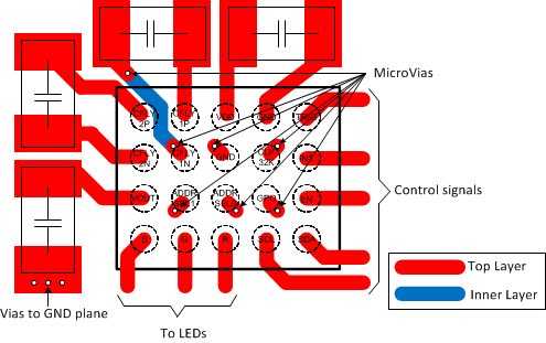
Place capacitors as close to the LP5521 device as possible to minimize the current loops. Figure 31 shows an example of LP5521 PCB layout and component placement.

Layout Example

LP5521 LP5521_layout_example.gif Figure 31. Example of Typical Layout