SNVS798P April   2012  – January 2024 LP5907

PRODUCTION DATA  

  1.   1
  2. Features
  3. Applications
  4. Description
  5. Pin Configuration and Functions
  6. Specifications
    1. 5.1 Absolute Maximum Ratings
    2. 5.2 ESD Ratings
    3. 5.3 Recommended Operating Conditions
    4. 5.4 Thermal Information
    5. 5.5 Electrical Characteristics
    6. 5.6 Output and Input Capacitors
    7. 5.7 Typical Characteristics
  7. Detailed Description
    1. 6.1 Overview
    2. 6.2 Functional Block Diagram
    3. 6.3 Feature Description
      1. 6.3.1 Enable (EN)
      2. 6.3.2 Low Output Noise
      3. 6.3.3 Output Automatic Discharge
      4. 6.3.4 Remote Output Capacitor Placement
      5. 6.3.5 Thermal Overload Protection (TSD)
    4. 6.4 Device Functional Modes
      1. 6.4.1 Enable (EN)
      2. 6.4.2 Minimum Operating Input Voltage (VIN)
  8. Application and Implementation
    1. 7.1 Application Information
    2. 7.2 Typical Application
      1. 7.2.1 Design Requirements
      2. 7.2.2 Detailed Design Procedure
        1. 7.2.2.1 Custom Design With WEBENCH® Tools
        2. 7.2.2.2 Power Dissipation and Device Operation
        3. 7.2.2.3 External Capacitors
        4. 7.2.2.4 Input Capacitor
        5. 7.2.2.5 Output Capacitor
        6. 7.2.2.6 Capacitor Characteristics
        7. 7.2.2.7 Remote Capacitor Operation
        8. 7.2.2.8 No-Load Stability
        9. 7.2.2.9 Enable Control
      3. 7.2.3 Application Curves
    3. 7.3 Power Supply Recommendations
    4. 7.4 Layout
      1. 7.4.1 Layout Guidelines
        1. 7.4.1.1 X2SON Mounting
        2. 7.4.1.2 DSBGA Mounting
        3. 7.4.1.3 DSBGA Light Sensitivity
      2. 7.4.2 Layout Examples
  9. Device and Documentation Support
    1. 8.1 Documentation Support
      1. 8.1.1 Custom Design With WEBENCH® Tools
      2. 8.1.2 Related Documentation
    2. 8.2 Receiving Notification of Documentation Updates
    3. 8.3 Support Resources
    4. 8.4 Trademarks
    5. 8.5 Electrostatic Discharge Caution
    6. 8.6 Glossary
  10. Revision History
  11. 10Mechanical, Packaging, and Orderable Information

Package Options

Refer to the PDF data sheet for device specific package drawings

Mechanical Data (Package|Pins)
  • YKM|4
  • DBV|5
  • DQN|4
  • YKG|4
  • YKE|4
Thermal pad, mechanical data (Package|Pins)
Orderable Information

Typical Characteristics

VIN = 3.7V, VOUT = 2.8V, IOUT = 1mA, CIN = 1µF, COUT = 1µF, and TA = 25°C (unless otherwise noted)
GUID-CE7D35D3-65DC-43E0-B095-6625155DB83C-low.gif
 
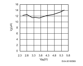
Figure 5-1 Quiescent Current vs Input Voltage
GUID-95695005-8C26-4760-A448-A09AC6F31911-low.gif
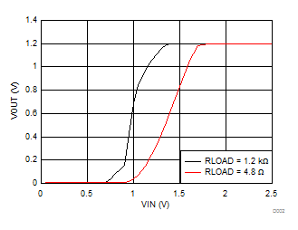
VOUT = 1.2V, VEN = VIN
Figure 5-3 VOUT vs VIN
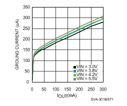
GUID-9DCC9967-0CD5-4600-8852-3187F5F4045D-low.gif
 
Figure 5-5 Ground Current vs Output Current
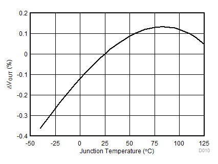
GUID-4840B747-4444-446B-9960-261322260666-low.gif
 
Figure 5-7 ΔVOUT vs Temperature
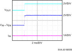
GUID-5F4A7FFF-3635-4B8E-9DC6-B308B403880E-low.gif
 
Figure 5-9 Inrush Current
GUID-D86BE94D-EB35-4134-AECE-44E928E72DE0-low.gif
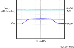
VIN = 3.2V ↔ 4.2V, load = 250mA
Figure 5-11 Line Transient
GUID-64F67B2B-B2CC-42D3-A8AC-87C59F89302F-low.gif
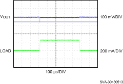
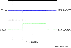
Load = 0mA ↔ 250mA, 90°C
Figure 5-13 Load Transient
GUID-47AE3B8C-9D40-424B-B74C-FB67FFE1D287-low.gif
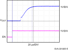
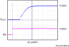
Load = 0mA
Figure 5-15 Start-Up
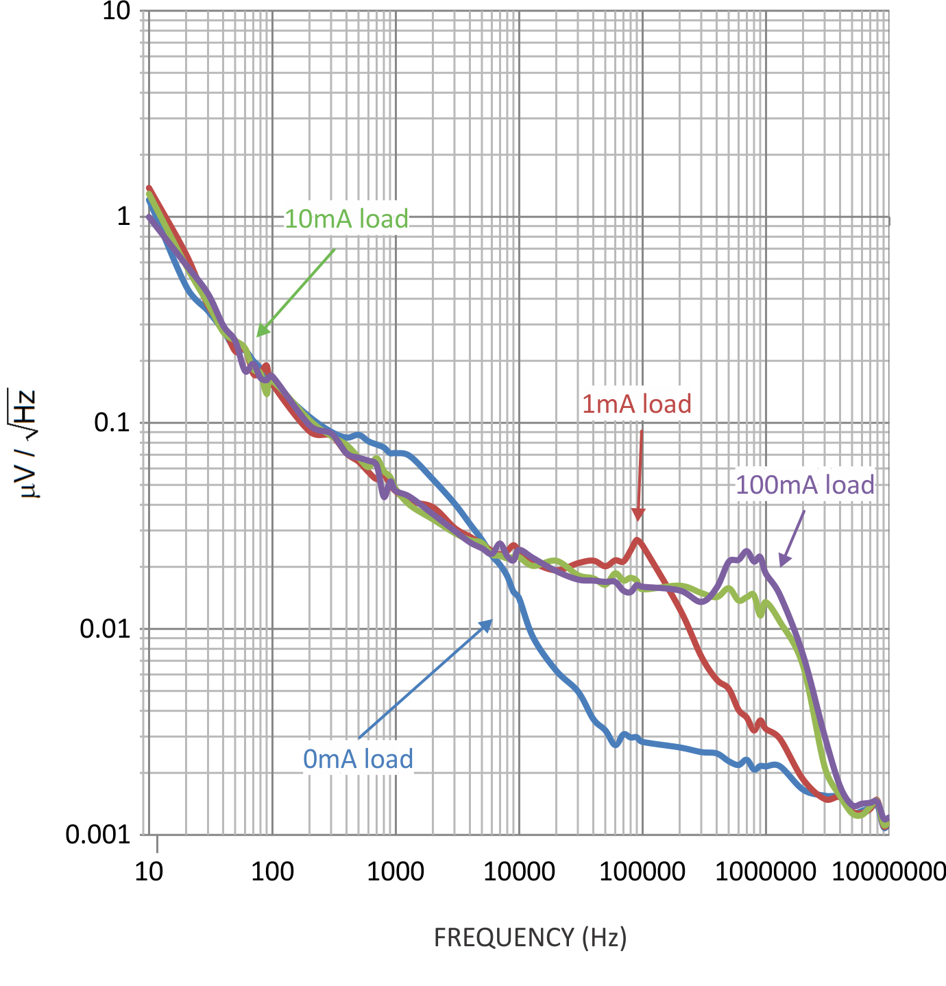
GUID-DC67695F-32DE-4AA1-BFB7-DA9639701730-low.png
 
Figure 5-17 Noise Density Test
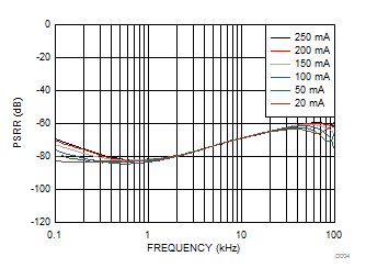
GUID-62E4DA5F-3150-4E99-A5B7-AEE77C98FF62-low.gif
 
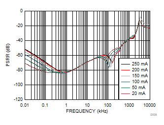
Figure 5-19 PSRR Loads Averaged 100Hz to 100kHz
GUID-DC18D5C7-776A-4ADF-9DF0-8E85CCB4B169-low.gif
 
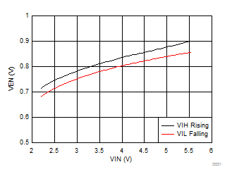
Figure 5-2 VEN Thresholds vs VIN
GUID-490736FB-5855-47D5-9524-65DEE979B8ED-low.gif
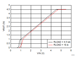
VOUT = 4.5V, VEN = VIN
Figure 5-4 VOUT vs VIN
GUID-D37ACCFB-CB64-447F-9A9F-7D42DFD2AC64-low.gif
 
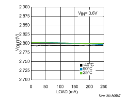
Figure 5-6 Load Regulation
GUID-14439F61-CF24-4164-9806-97BDC407F77D-low.gif
 
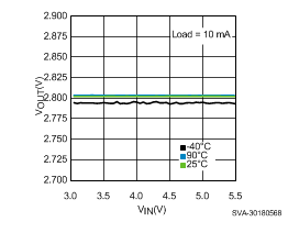
Figure 5-8 Line Regulation
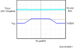
GUID-3B42AA98-03D4-4C67-82DA-CB1A65636EDE-low.gif
VIN = 3.2V ↔ 4.2V, load = 1mA
Figure 5-10 Line Transient
GUID-8B06B405-6B59-46D7-AE54-4742DB425CA3-low.gif
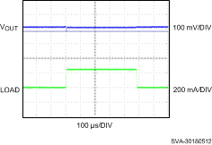
Load = 0mA ↔ 250mA, –40°C
Figure 5-12 Load Transient
GUID-522734A2-72D2-4B3E-A175-9C3F143ACBC2-low.gif
Load = 0mA ↔ 250mA, 25°C
Figure 5-14 Load Transient
GUID-42B3626B-CC7B-4608-B883-CEEB8A918404-low.gif
Load = 250mA
Figure 5-16 Start-Up
GUID-2584CC18-0935-4433-984F-E249BA96AF31-low.gif
 
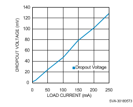
Figure 5-18 Dropout Voltage vs Load Current
GUID-8D0396E3-A1C3-48D4-8F10-571C3F60340F-low.gif
 
Figure 5-20 PSRR Loads Averaged 10Hz to 10MHz