SNVS693E September 2011 – September 2014 LP8552
PRODUCTION DATA.
- 1 Features
- 2 Applications
- 3 Description
- 4 Revision History
- 5 Default EEPROM Values
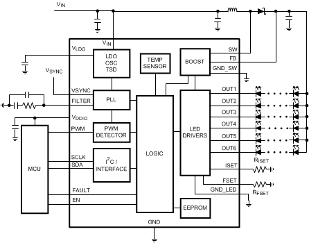
- 6 Pin Configuration and Functions
-
7 Specifications
- 7.1 Absolute Maximum Ratings
- 7.2 Handling Ratings
- 7.3 Recommended Operating Conditions
- 7.4 Thermal Information
- 7.5 Electrical Characteristics
- 7.6 Boost Converter Electrical Characteristics
- 7.7 LED Driver Electrical Characteristics
- 7.8 PWM Interface Characteristics
- 7.9 Undervoltage Protection
- 7.10 Logic Interface Characteristics
- 7.11 I2C Serial Bus Timing Parameters (SDA, SCLK)
- 7.12 Typical Characteristics
-
8 Detailed Description
- 8.1 Overview
- 8.2 Functional Block Diagram
- 8.3
Feature Description
- 8.3.1 Clock Generation
- 8.3.2
Brightness Control Methods
- 8.3.2.1 PWM Input Duty Cycle
- 8.3.2.2 Brightness Register Control
- 8.3.2.3 PWM Direct Control
- 8.3.2.4 PWM Calculation Data Flow
- 8.3.2.5 PWM Detector
- 8.3.2.6 Brightness Control
- 8.3.2.7 Resolution Selector
- 8.3.2.8 Sloper
- 8.3.2.9 PWM & Current Control
- 8.3.2.10 Dither
- 8.3.2.11 PWM Comparator
- 8.3.2.12 Current Setting
- 8.3.2.13 PWM Frequency Setting
- 8.3.2.14 Phase Shift PWM Scheme
- 8.3.2.15 Slope And Dithering
- 8.3.2.16 Driver Headroom Control
- 8.3.3 Boost Converter
- 8.3.4 Fault Detection
- 8.4 Device Functional Modes
- 8.5 Programming
- 8.6 Register Maps
- 9 Application and Implementation
- 10Power Supply Recommendations
- 11Layout
- 12Device and Documentation Support
- 13Mechanical, Packaging, and Orderable Information
Package Options
Mechanical Data (Package|Pins)
- YZR|25
Thermal pad, mechanical data (Package|Pins)
Orderable Information
8 Detailed Description
8.1 Overview
LP8552 is a high-voltage LED driver for medium sized LCD backlight applications. It includes high-voltage boost converter. Boost voltage automatically sets to the correct level needed to drive the LED strings. This is done by monitoring LED output voltage drop in real time.
Six LED outputs are driven either with constant current sinks with PWM control or by controlling both PWM and current. Constant current value is set with EEPROM bits and with RISET resistor. Brightness (PWM) is controlled either with I2C register or with PWM input. PWM frequencies are set with EEPROM bits and with RFSET resistor. Special Phase-Shift PWM mode can be used to reduce boost output current peak, thus reducing output ripple, capacitor size and audible noise.
With LP8552 it is possible to synchronize the PWM output frequency to VSYNC signal received from video processor. Internal PLL ensures that the PWM output clock is always synchronized to the VSYNC signal.
Special dithering mode makes it possible to increase output resolution during fading between two brightness values and by this making the transition look very smooth with virtually no stepping. Transition slope time can be adjusted with EEPROM bits.
Safety features include LED fault detection with open and short detection. LED fault detection will prevent system overheating in case of open in some of the LED strings. Chip internal temperature is constantly monitored and based on this LP8552 can reduce the brightness of the backlight to reduce thermal loading once certain trip point is reached. Threshold is programmable in EEPROM. If chip internal temperature reaches too high, the boost converter and LED outputs are completely turned off until the internal temperature has reached acceptable level. Boost converter is protected against too high load current and over-voltage. LP8552 notifies the system about the fault through I2C register and with FAULT pin.
EEPROM programmable functions include:
- PWM frequencies
- Phase shift PWM mode
- LED constant current
- Boost output frequency
- Temperature thresholds
- Slope for brightness changes
- Dithering options
- PWM output resolution
- Boost control bits
External components RISET and RFSET can also be used for selecting the output current and PWM frequencies.
8.2 Functional Block Diagram
8.3 Feature Description
8.3.1 Clock Generation
The LP8552 has an internal 5-MHz oscillator which is used for clocking the boost converter, state machine, PWM input duty cycle measurement, internal timings such as slope time for output brightness changes.
The internal clock can be used for generating the PWM output frequency. In this case the 5-MHz clock can be multiplied with the internal PLL to achieve higher resolution. The higher the clock frequency for PWM generation block, the higher the resolution; however, the tradeoff is higher IQ of the part. Clock multiplication is set with <PWM_RESOLUTION[1:0]> EEPROM Bits.
The PLL can also be used for generating the required PWM generation clock from the VSYNC signal. This makes sure that the LED output PWM is always synchronized to the VSYNC signal and there is no clock variation between LCD display video update and the LED backlight output frequency. Also HSYNC signal up to 55 kHz can be used.
PLL has an internal counter which has 13-bit control <PLL[12:0]> to achieve correct output clock frequency based on the VSYNC frequency.
For the PLL it can take couple of seconds to synchronize the VSYNC signal to 60 Hz in start-up before the correct PWM clock frequency is generated from internal oscillator. FILTER pin component selection affects the time it takes from the PLL to lock to VSYNC signal.
Special logic is implemented for allowing steady clock frequency even if there are missing VSYNC pulses. In case pulses are randomly left out, the LP8552 can generate the pulses internally while keeping the same PWM output frequency. When VSYNC pulses are available again, the internal logic will automatically switch to the external VSYNC clock without glitch.
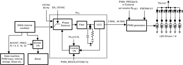 Figure 12. Principle Of The Clock Generation
8.3.2 Brightness Control Methods
LP8552 controls the brightness of the backlight with PWM. PWM control is received either from PWM input pin or from I2C register bits. The PWM source selection is done with <BRT_MODE[1:0]> bits:
| BRT_MODE[1] | BRT_MODE[0] | PWM SOURCE |
|---|---|---|
| 0 | 0 | PWM input pin duty cycle control. Default. |
| 0 | 1 | PWM input pin duty cycle control. |
| 1 | 0 | Brightness register |
| 1 | 1 | PWM direct control (PWM in = PWM out) |
8.3.2.1 PWM Input Duty Cycle
With PWM input pin duty cycle control the output PWM is controlled by PWM input duty cycle. PWM detector block measures the duty cycle in the PWM pin and uses this 13-bit value to generate the output PWM. Output PWM can have different frequency than input in this mode, and also phase shift PWM mode can be used. Slope and dither are effective in this mode. PWM input resolution is defined by the input PWM clock frequency.
8.3.2.2 Brightness Register Control
With brightness register control the output PWM is controlled with 8-bit resolution <BRT7:0> register bits. Phase shift scheme can be used with this, and the output PWM frequency can be freely selected. Slope and dither are effective in this mode.
8.3.2.3 PWM Direct Control
With PWM direct control the output PWM will directly follow the input PWM. Due to the internal logic structure the input is anyway clocked with the 5-MHz clock or the PLL clock. PSPWM mode is not possible in this mode. Slope and dither are not effective in this mode.
8.3.2.4 PWM Calculation Data Flow
Figure 13 is a flow chart of the PWM calculation data flow. In PWM direct control mode most of the blocks are bypassed, and this flow chart does not apply.
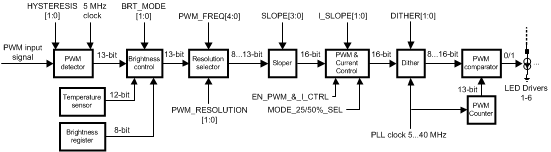 Figure 13. PWM Calculation Data Flow
8.3.2.5 PWM Detector
The PWM detector block measures the duty cycle of the input PWM signal. Resolution depends on the input signal frequency. Hysteresis selection sets the minimum allowable change to the input. If smaller change is detected, it is ignored. With hysteresis the constant changing between two brightness values is avoided if there is small jitter in the input signal.
8.3.2.6 Brightness Control
Brightness control block gets the13-bit value from the PWM detector, 12-bit value from the temperature sensor, as well as 8-bit value from the brightness register. <BRT_MODE[1:0]> selects whether to use PWM input duty cycle value or the brightness register value as described earlier. Based on the temperature sensor value the duty cycle is reduced if the temperature has reached the temperature limit set to the <TEMP_LIM[1:0]> EEPROM bits.
8.3.2.7 Resolution Selector
Resolution selector takes the necessary MSB bits from the input data to match the output resolution. For example, if 11-bit resolution is used for output, then 11 MSB bits are selected from the input. Dither bits are not taken into account for the output resolution. This is to make sure that in steady state condition, there is no dithering used for the output.
8.3.2.8 Sloper
Sloper makes the smooth transition from one brightness value to another. Slope time can be adjusted from 0 to 500 ms with <SLOPE[3:0]> EEPROM bits. The sloper output is 16-bit value.
8.3.2.9 PWM & Current Control
Automatic PWM & current control improves the optical efficiency of the LEDs by using PWM control with small brightness values and current control with bigger values. <EN_PWM_&_I_CTRL > EEPROM bit selects whether the PWM & current control is used instead of PWM control or not. PWM to current dimming switch point can be set to 25% or 50% of the brightness range with <MODE_25/50_SEL> EEPROM bit. Current slope can be adjusted by using the <I_SLOPE[1:0]> EEPROM bits.
8.3.2.10 Dither
With dithering the output resolution can be “artificially” increased during sloping from one brightness value to another. This way the brightness change steps are not visible to eye. Dithering can be from 0 to 3 bits, and is selected with <DITHER[1:0]> EEPROM bits.
8.3.2.11 PWM Comparator
The PWM counter clocks the PWM comparator based on the duty-cycle value received from Dither block. Output of the PWM comparator controls directly the LED drivers. If PSPWM mode is used, then the signal to each LED output is delayed certain amount.
8.3.2.12 Current Setting
Maximum current of the LED outputs is controlled with CURRENT[7:0] EEPROM register bits linearly from 0 to 30 mA. If <EN_I_RES> = 1 the maximum LED output current can be scaled also with external resistor, RISET. RISET controls the LED current as shown in Equation 1:

Default value for CURRENT[7:0] = 7Fh (127d). Therefore, the output current can be calculated as shown in Equation 2:

For example, if a 16-kΩ RISET resistor is used, then the LED maximum current is 23 mA. Note that formula is only approximation for the actual current.
8.3.2.13 PWM Frequency Setting
PWM frequency is selected with PWM_FREQ[4:0] EEPROM register. If PLL clock frequency multiplication is used, it will affect the output PWM frequency as well. <PWM_RESOLUTION[1:0]> EEPROM bits will select the PLL output frequency and hence the PWM frequency and resolution. Below are listed PWM frequencies with <EN_VSYNC]> = 0. PWM resolution setting affects the PLL clock frequency (5 MHz to 40 MHz). Highlighted frequencies with boldface can be selected also with external resistor RFSET. To activate RFSET frequency selection the <EN_F_RES> EEPROM bit must be 1.
Table 1. Available PWM Frequencies and Resolutions
| PWM_RES[1:0] | 00 | 01 | 10 | 11 | |
|---|---|---|---|---|---|
| PWM_FREQ[4:0] | 5 MHz | 10 MHz | 20 MHz | 40 MHz | RESOLUTION (bits) |
| 11111 | 19232 | - | - | - | 8 |
| 11110 | 16828 | - | - | - | 8 |
| 11101 | 14424 | - | - | - | 8 |
| 11100 | 12020 | - | - | - | 8 |
| 11011 | 9616 | 19232 | - | - | 9 |
| 11010 | 7963 | 15927 | - | - | 9 |
| 11001 | 6386 | 12771 | - | - | 9 |
| 11000 | 4808 | 9616 | 19232 | - | 10 |
| 10111 | 4658 | 9316 | 18631 | - | 10 |
| 10110 | 4508 | 9015 | 18030 | - | 10 |
| 10101 | 4357 | 8715 | 17429 | - | 10 |
| 10100 | 4207 | 8414 | 16828 | - | 10 |
| 10011 | 4057 | 8114 | 16227 | - | 10 |
| 10010 | 3907 | 7813 | 15626 | - | 10 |
| 10001 | 3756 | 7513 | 15025 | - | 10 |
| 10000 | 3606 | 7212 | 14424 | - | 10 |
| 01111 | 3456 | 6912 | 13823 | - | 10 |
| 01110 | 3306 | 6611 | 13222 | - | 10 |
| 01101 | 3155 | 6311 | 12621 | - | 10 |
| 01100 | 3005 | 6010 | 12020 | - | 10 |
| 01011 | 2855 | 5710 | 11419 | - | 10 |
| 01010 | 2705 | 5409 | 10818 | - | 10 |
| 01001 | 2554 | 5109 | 10217 | - | 10 |
| 01000 | 2404 | 4808 | 9616 | 19232 | 11 |
| 00111 | 2179 | 4357 | 8715 | 17429 | 11 |
| 00110 | 1953 | 3907 | 7813 | 15626 | 11 |
| 00101 | 1728 | 3456 | 6912 | 13823 | 11 |
| 00100 | 1503 | 3005 | 6010 | 12020 | 11 |
| 00011 | 1202 | 2404 | 4808 | 9616 | 12 |
| 00010 | 1052 | 2104 | 4207 | 8414 | 12 |
| 00001 | 826 | 1653 | 3306 | 6611 | 12 |
| 00000 | 601 | 1202 | 2404 | 4808 | 13 |
RFSET resistance values with corresponding PWM frequencies:
Table 2. PWM Frequency Selection with Resistor
| PWM_RES[1:0] | 00 | 01 | 10 | 11 | ||||
|---|---|---|---|---|---|---|---|---|
| RFSET (kΩ) | 5 MHz CLOCK | RESOLUTION | 10 MHz CLOCK | RESOLUTION | 20 MHz CLOCK | RESOLUTION | 40 MHz CLOCK | RESOLUTION |
| 10...15 | 19232 | 8 | 19232 | 9 | 19232 | 10 | 19232 | 11 |
| 26...29 | 16828 | 8 | 15927 | 9 | 16227 | 10 | 17429 | 11 |
| 36...41 | 14424 | 8 | 12771 | 9 | 14424 | 10 | 15626 | 11 |
| 50...60 | 12020 | 8 | 9616 | 10 | 12020 | 10 | 12020 | 11 |
| 85...100 | 9616 | 9 | 8715 | 10 | 9616 | 11 | 9616 | 12 |
| 135...150 | 7963 | 9 | 7813 | 10 | 7813 | 11 | 8414 | 12 |
| 200...300 | 6386 | 9 | 6311 | 10 | 6010 | 11 | 6811 | 12 |
| 450... | 4808 | 10 | 4808 | 11 | 4808 | 12 | 4808 | 13 |
8.3.2.14 Phase Shift PWM Scheme
Phase shift PWM scheme allows delaying the time when each LED output is active. When the LED output are not activated simultaneously, the peak load current from the boost output is greatly decreased. This reduces the ripple seen on the boost output and allows smaller output capacitors. Reduced ripple also reduces the output ceramic capacitor audible ringing. PSPWM scheme also increases the load frequency seen on boost output by x6 and therefore transfers the possible audible noise to so high frequency that human ear cannot hear it.
Description of the PSPWM mode is seen in Figure 14. PSPWM mode is enabled by setting <EN_PSPWM> EEPROM bit to 1. Shift time is the delay between outputs and it is defined as 1 / (fPWM x 6). If the <EN_PSPWM> bit is 0, then the delay is 0 and all outputs are active simultaneously.
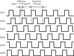 Figure 14. Phase Shift PWM Mode
8.3.2.15 Slope And Dithering
During transition between two brightness (PWM) values special dithering scheme is used if the slope is enabled. It allows increased resolution and smaller average steps size. Dithering is not used in steady state condition. Slope time can be programmed with EEPROM bits <SLOPE[3:0]> from 0 to 500 ms. Same slope time is used for sloping up and down. Advanced slope makes brightness changes smooth for eye. Dithering can be programmed with EEPROM bits <DITHER[1:0]> from 0 to 3 bits. Figure 16 below is for 1-bit dithering; for 3-bit dithering, every 8th pulse is made 1 LSB longer to increase the average value by 1/8 of LSB.
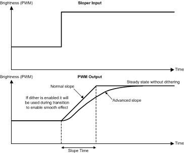 Figure 15. Sloper Operation
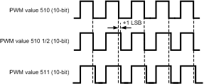 Figure 16. Example Of The Dithering, 1-Bit Dither, 10-Bit Resolution
8.3.2.16 Driver Headroom Control
Driver headroom can be controlled with <DRV_HEADR[2:0]> EEPROM bits. Driver headroom control sets the minimum threshold for the voltage over the LED output which has the smallest driver headroom and controls the boost output voltage accordingly. Boost output voltage step size is 125 mV. The LED output which has the smallest forward voltage is the one which has highest VF across the LEDs. The strings with highest forward voltage is detected automatically. To achieve best possible efficiency smallest possible headroom voltage should be selected. If there is high variation between LED strings, the headroom can be raised slightly to prevent any visual artifacts.
8.3.3 Boost Converter
8.3.3.1 Operation
The LP8552 boost DC/DC converter generates a 10-V to 40-V supply voltage for the LEDs from 2.7-V to 22-V input voltage. The output voltage can be controlled either with EEPROM register bits <VBOOST[4:0]>, or automatic adaptive voltage control can be used. The converter is a magnetic-switching PWM mode DC/DC converter with a current limit. The topology of the magnetic boost converter is called CPM (current programmed mode) control, where the inductor current is measured and controlled with the feedback. Switching frequency is selectable between 156 kHz and 1.25 MHz with EEPROM bit <BOOST_FREQ[1:0]>. When <EN_BOOST> EEPROM register bit is set to 1, then boost will activate automatically when backlight is enabled.
In adaptive mode the boost output voltage is adjusted automatically based on LED driver headroom voltage. Boost output voltage control step size is in this case 125 mV to ensure as small as possible driver headroom and high efficiency. Enabling the adaptive mode is done with <EN_ADAPT> EEPROM bit. If boost is started with adaptive mode enabled, then the initial boost output voltage value is defined with the <VBOOST[4:0]> EEPROM register bits in order to eliminate long output voltage iteration time when boost is started for the first time. Figure 17 shows the boost topology with the protection circuitry:
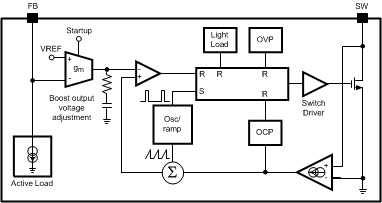 Figure 17. Boost Topology with Protection Circuitry
8.3.3.2 Protection
Three different protection schemes are implemented:
- Overvoltage protection, limits the maximum output voltage.
- Overvoltage protection limit changes dynamically based on output voltage setting.
- Keeps the output below breakdown voltage
- Prevents boost operation if battery voltage is much higher than desired output.
- Overcurrent protection, limits the maximum inductor current.
- Duty cycle limiting.
8.3.3.3 Manual Output Voltage Control
User can control the boost output voltage with <VBOOST[4:0]> EEPROM register bits when adaptive mode is disabled.
| VBOOST[4:0] | VOLTAGE (typical) | |
|---|---|---|
| Bin | Dec | Volts |
| 00000 | 0 | 10 |
| 00001 | 1 | 11 |
| 00010 | 2 | 12 |
| 00011 | 3 | 13 |
| 00100 | 4 | 14 |
| ... | ... | ... |
| 11101 | 29 | 39 |
| 11110 | 30 | 40 |
| 11111 | 31 | 40 |
8.3.3.4 Adaptive Boost Control
Adaptive boost control function adjusts the boost output voltage to the minimum sufficient voltage for proper LED driver operation. The output with highest VF LED string is detected and boost output voltage adjusted accordingly. Driver headroom can be adjusted with <DRIVER_HEADR[2:0]> EEPROM bits from approximately 300 mV to 1200 mV. Boost adaptive control voltage step size is 125 mV. Boost adaptive control operates similarly with and without PSPWM.
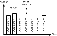 Figure 18. Boost Adaptive Control Principle With PSPWM
8.3.4 Fault Detection
The LP8552 has fault detection for LED fault, low-battery voltage, overcurrent, and thermal shutdown. The open drain output pin (FAULT) can be used to indicate occurred fault. The cause for the fault can be read from status register. Reading the fault register will also reset the fault. Setting the EN pin low will also reset the faults, even if an external 5V line is used to power VLDO pin.
8.3.4.1 LED Fault Detection
With LED fault detection, the voltages across the LED drivers are constantly monitored. Shorted or open LED string is detected.
If LED fault is detected:
- The corresponding LED string is taken out of boost adaptive control loop;
- Fault bits are set in the fault register to identify whether the fault has been open/short and how many strings are faulty; and
- Fault open-drain pin is pulled down.
LED fault sensitivity can be adjusted with <LED_FAULT_THR> EEPROM bit which sets the allowable variation between LED output voltage to 3.3 V or 5.3 V. Depending on application, and how much variation there can be in normal operation between LED string forward voltages, this setting can be adjusted.
Fault is cleared by setting EN pin low or by reading the fault register.
By default the LED fault detection is active only in automatic PWM & current dimming mode. If LED fault detection is needed in PWM dimming mode, please contact a Texas Instruments representative for guidance.
8.3.4.2 Undervoltage Detection
LP8552 has detection for too-low VIN voltage. Threshold level for the voltage is set with EEPROM register bits as seen in Table 3:
Table 3. Threshold Level for Voltage Set with EEPROM Register Bits
| UVLO[1:0] | THRESHOLD (V) |
|---|---|
| 00 | OFF |
| 01 | 2.7 |
| 10 | 5.4 |
| 11 | 8.1 |
When undervoltage is detected the LED outputs and boost will shutdown, FAULT pin is pulled down and corresponding fault bit is set in fault register. LEDs and boost will start again when the voltage has increased above the threshold level. Hysteresis is implemented to threshold level to avoid continuous triggering of fault when threshold is reached.
Fault is cleared by setting EN pin low or by reading the fault register.
8.3.4.3 Overcurrent Protection
The device has detection for too-high loading on the boost converter. When overcurrent fault is detected, the LP8552 will shut down.
Fault is cleared by setting EN pin low or by reading the fault register.
8.3.4.4 Device Thermal Regulation
The LP8552 has an internal temperature sensor which can be used to measure the junction temperature of the device and protect the device from overheating. During thermal regulation, LED PWM is reduced by 2% of full scale per °C whenever the temperature threshold is reached. Temperature regulation is enabled automatically when chip is enabled. 11-bit temperature value can be read from Temp MSB and Temp LSB registers; MSB should be read first. Temperature limit can be programmed in EEPROM as shown in Table 4.
Thermal regulation function does not generate fault signal.
Table 4. Temperature Limits Programmable in EEPROM
| TEMP_LIM[1:0] | OVER-TEMP LIMIT (°C) |
|---|---|
| 00 | OFF |
| 01 | 110 |
| 10 | 120 |
| 11 | 130 |
8.3.4.5 Thermal Shutdown
If the LP8552 reaches thermal shutdown temperature (150°C) the LED outputs and boost will shut down to protect it from damage. Also, the fault pin will be pulled down to indicate the fault state. Device will activate again when temperature drops below 130°C degrees.
Fault is cleared by setting EN pin low or by reading the fault register.
8.4 Device Functional Modes
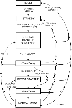 Figure 19. Device Functional Modes
-
RESET:In the RESET mode all the internal registers are reset to the default values. Reset is entered always when VLDO voltage is low. EN pin is enable for the internal LDO. Power On Reset (POR) activates during the chip startup or when the supply voltage VLDO falls below POR level. Once VLDO rises above POR level, POR will inactivate, and the chip will continue to the STANDBY mode.
-
STANDBY:The STANDBY mode is entered if the register bit BL_CTL is LOW and external PWM input is not active and POR is not active. This is the low power consumption mode, when only internal 5-V LDO is enabled. Registers can be written in this mode, and the control bits are effective immediately after start-up.
-
START-UP:When BL_CTL bit is written high or PWM signal is high, the INTERNAL START-UP SEQUENCE powers up all the needed internal blocks (VREF, Bias, Oscillator etc.). Internal EPROM and EEPROM are read in this mode. To ensure the correct oscillator initialization, etc., a 2-ms delay is generated by the internal state-machine. If the chip temperature rises too high, the Thermal Shutdown (TSD) disables the chip operation and STARTUP mode is entered until no thermal shutdown event is present.
-
BOOST START-UP:Soft start for boost output is generated in the BOOST START-UP mode. The boost output is raised in low current PWM mode during the 4 ms delay generated by the state-machine. All LED outputs are off during the 4-ms delay to ensure smooth start-up. The Boost start-up is entered from Internal Start-up Sequence if EN_BOOST is HIGH.
-
NORMAL:During NORMAL mode the user controls the chip using the external PWM input or with Control Registers through I2C. The registers can be written in any sequence and any number of bits can be altered in a register in one write.
8.5 Programming
8.5.1 I2C-Compatible Serial Bus Interface
8.5.1.1 Interface Bus Overview
The I2C-compatible synchronous serial interface provides access to the programmable functions and registers on the device. This protocol uses a two-wire interface for bidirectional communications between the ICs connected to the bus. The two interface lines are the Serial Data Line (SDA) and the Serial Clock Line (SCLK). These lines should be connected to a positive supply, via a pull-up resistor and remain HIGH even when the bus is idle.
Every device on the bus is assigned a unique address and acts as either a Master or a Slave depending on whether it generates or receives the SCLK. The LP8552 is always a slave device.
8.5.1.2 Data Transactions
One data bit is transferred during each clock pulse. Data is sampled during the high state of the serial clock SCLK. Consequently, throughout the clock’s high period, the data should remain stable. Any changes on the SDA line during the high state of the SCLK and in the middle of a transaction, aborts the current transaction. New data should be sent during the low SCLK state. This protocol permits a single data line to transfer both command/control information and data using the synchronous serial clock.
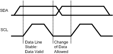 Figure 20. Bit Transfer
Each data transaction is composed of a Start Condition, a number of byte transfers (set by the software) and a Stop Condition to terminate the transaction. Every byte written to the SDA bus must be 8 bits long and is transferred with the most significant bit first. After each byte, an Acknowledge signal must follow as described in below sections.
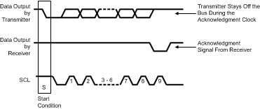 Figure 21. Start and Stop
The Master device on the bus always generates the Start and Stop Conditions (control codes). After a Start Condition is generated, the bus is considered busy and it retains this status until a certain time after a Stop Condition is generated. A high-to-low transition of the data line (SDA) while the clock (SCLK) is high indicates a Start Condition. A low-to-high transition of the SDA line while the SCLK is high indicates a Stop Condition.
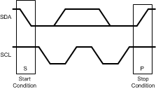 Figure 22. Start and Stop Conditions
In addition to the first Start Condition, a repeated Start Condition can be generated in the middle of a transaction. This allows another device to be accessed, or a register read cycle.
8.5.1.3 Acknowledge Cycle
The Acknowledge Cycle consists of two signals: the acknowledge clock pulse the master sends with each byte transferred, and the acknowledge signal sent by the receiving device.
The master generates the acknowledge clock pulse on the ninth clock pulse of the byte transfer. The transmitter releases the SDA line (permits it to go high) to allow the receiver to send the acknowledge signal. The receiver must pull down the SDA line during the acknowledge clock pulse and ensure that SDA remains low during the high period of the clock pulse, thus signaling the correct reception of the last data byte and its readiness to receive the next byte.
8.5.1.4 “Acknowledge After Every Byte” Rule
The master generates an acknowledge clock pulse after each byte transfer. The receiver sends an acknowledge signal after every byte received.
There is one exception to the “acknowledge after every byte” rule. When the master is the receiver, it must indicate to the transmitter an end of data by not-acknowledging (“negative acknowledge”) the last byte clocked out of the slave. This “negative acknowledge” still includes the acknowledge clock pulse (generated by the master), but the SDA line is not pulled down.
8.5.1.5 Addressing Transfer Formats
Each device on the bus has a unique slave address. The LP8552 operates as a slave device with 7-bit address combined with data direction bit. Slave address is 2Ch as 7-bit or 58h for write and 59h for read in 8-bit format.
Before any data is transmitted, the master transmits the address of the slave being addressed. The slave device should send an acknowledge signal on the SDA line, once it recognizes its address.
The slave address is the first seven bits after a Start Condition. The direction of the data transfer (R/W) depends on the bit sent after the slave address — the eighth bit.
When the slave address is sent, each device in the system compares this slave address with its own. If there is a match, the device considers itself addressed and sends an acknowledge signal. Depending upon the state of the R/W bit (1:read, 0:write), the device acts as a transmitter or a receiver.
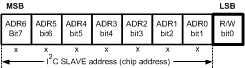 Figure 23. I2C Chip Address
8.5.1.6 Control Register Write Cycle
- Master device generates start condition.
- Master device sends slave address (7 bits) and the data direction bit (r/w = 0).
- Slave device sends acknowledge signal if the slave address is correct.
- Master sends control register address (8 bits).
- Slave sends acknowledge signal.
- Master sends data byte to be written to the addressed register.
- Slave sends acknowledge signal.
- If master sends further data bytes the control register address is incremented by one after acknowledge signal.
- Write cycle ends when the master creates stop condition.
8.5.1.7 Control Register Read Cycle
- Master device generates a start condition.
- Master device sends slave address (7 bits) and the data direction bit (r/w = 0).
- Slave device sends acknowledge signal if the slave address is correct.
- Master sends control register address (8 bits).
- Slave sends acknowledge signal.
- Master device generates repeated start condition.
- Master sends the slave address (7 bits) and the data direction bit (r/w = 1).
- Slave sends acknowledge signal if the slave address is correct.
- Slave sends data byte from addressed register.
- If the master device sends acknowledge signal, the control register address is incremented by one. Slave device sends data byte from addressed register.
- Read cycle ends when the master does not generate acknowledge signal after data byte and generates stop condition.
Table 5. Data Read and Write Cycles
| ADDRESS MODE | |
|---|---|
| Data Read | <Start Condition> <Slave Address><r/w = 0>[Ack] <Register Addr.>[Ack] <Repeated Start Condition> <Slave Address><r/w = 1>[Ack] [Register Data]<Ack or NAck> … additional reads from subsequent register address possible <Stop Condition> |
| Data Write | <Start Condition> <Slave Address><r/w=’0’>[Ack] <Register Addr.>[Ack] <Register Data>[Ack] … additional writes to subsequent register address possible <Stop Condition> |
<>Data from master [ ] Data from slave
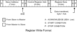 Figure 24. Register Write
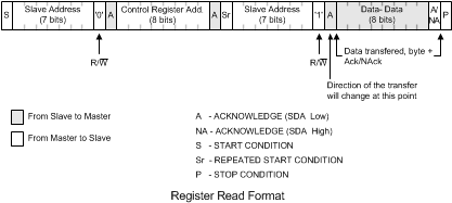 Figure 25. Register Read
8.5.2 EEPROM
EEPROM memory stores various parameters for chip control. The 64-bit EEPROM memory is organized as 8 x 8 bits. The EEPROM structure consists of a register front-end and the non-volatile memory (NVM). Register data can be read and written through the serial interface, and data is effective immediately. To read and program NVM, separate commands need to be sent. Erase and program voltages are generated on-chip charge pump, no other voltages than normal input voltage are required. A complete EEPROM memory map is shown in Table 7.
NOTE
EEPROM NVM can be programmed or read by customer for bench validation. Programming for production devices should be done in TI production test, where appropriate checks are performed to confirm EEPROM validity. Writing to EEPROM Control register of production devices (for burning or reading EEPROM) is not recommended. If special EEPROM configuration is required, please contact the TI Sales Office for availability.
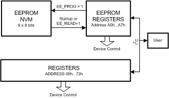 Figure 26. EEPROM Control Structure
8.6 Register Maps
Table 6. Register Map
| ADDR | REGISTER | D7 | D6 | D5 | D4 | D3 | D2 | D1 | D0 | DEFAULT |
|---|---|---|---|---|---|---|---|---|---|---|
| 00H | Brightness Control | BRT[7:0] | 0000 0000 | |||||||
| 01H | Device Control | BRT_MODE[1:0] | BL_CTL | 0000 0000 | ||||||
| 02H | Fault | OPEN | SHORT | 2_CHANNELS | 1_CHANNEL | BL_FAULT | OCP | TSD | UVLO | 0000 0000 |
| 03H | ID | PANEL | MFG[3:0] | REV[2:0] | 1111 1100 | |||||
| 04H | Direct Control | OUT[6:1] | 0000 0000 | |||||||
| 05H | Temp MSB | TEMP[10:3] | 0000 0000 | |||||||
| 06H | Temp LSB | TEMP[2:0] | 0000 0000 | |||||||
| 72H | EEPROM_control | EE_READY | EE_INIT | EE_PROG | EE_READ | 0000 0000 | ||||
8.6.1 Register Bit Explanations
8.6.1.1 Brightness Control
Address 00h
Reset value 0000 0000b
| BRIGHTNESS CONTROL REGISTER | |||||||
|---|---|---|---|---|---|---|---|
| 7 | 6 | 5 | 4 | 3 | 2 | 1 | 0 |
| BRT[7:0] | |||||||
| Name | Bit | Access | Description | ||||
| BRT | 7:0 | R/W | Backlight PWM 8-bit linear control. | ||||
8.6.1.2 Device Control
Address 01h
Reset value 0000 0000b
| DEVICE CONTROL REGISTER | |||||||
|---|---|---|---|---|---|---|---|
| 7 | 6 | 5 | 4 | 3 | 2 | 1 | 0 |
| BRT_MODE[1:0] | BL_CTL | ||||||
| Name | Bit | Access | Description | ||||
| BRT_MODE | 2:1 | R/W | PWM source mode | ||||
| 00b = PWM input pin duty cycle control (default) | |||||||
| 01b = PWM input pin duty cycle control | |||||||
| 10b = Brightness register | |||||||
| 11b = Direct PWM control from PWM input pin | |||||||
| BL_CTL | 0 | R/W | Enable backlight | ||||
| 0 = Backlight disabled and chip turned off if BRT_MODE[1:0] = 10. In external PWM pin control the state of the chip is defined with the PWM pin and this bit has no effect. | |||||||
| 1 = Backlight enabled and chip turned on if BRT_MODE[1:0] = 10. In external PWM pin control the state of the chip is defined with the PWM pin and this bit has no effect. | |||||||
8.6.1.3 Fault
Address 02h
Reset value 0000 0000b
| Fault register | |||||||
|---|---|---|---|---|---|---|---|
| 7 | 6 | 5 | 4 | 3 | 2 | 1 | 0 |
| OPEN | SHORT | 2_CHANNELS | 1_CHANNEL | BL_FAULT | OCP | TSD | UVLO |
| Name | Bit | Access | Description | ||||
| OPEN | 7 | R | LED open fault detection | ||||
| 0 = No fault | |||||||
| 1 = LED open fault detected. Fault pin is pulled to GND. Fault is cleared by reading the register 02h or setting EN pin low. | |||||||
| SHORT | 6 | R | LED short fault detection | ||||
| 0 = No fault | |||||||
| 1 = LED short fault detected. Fault pin is pulled to GND. Fault is cleared by reading the register 02h or setting EN pin low. | |||||||
| 2_CHANNELS | 5 | R | LED fault detection | ||||
| 0 = No fault | |||||||
| 1 = 2 or more channels have generated either short or open fault. Fault pin is pulled to GND. Fault is cleared by reading the register 02h or setting EN pin low. | |||||||
| 1_CHANNEL | 4 | R | LED fault detection | ||||
| 0 = No fault | |||||||
| 1 = 1 channel has generated either short or open fault. Fault pin is pulled to GND. Fault is cleared by reading the register 02h or setting EN pin low. | |||||||
| BL_FAULT | 3 | R | LED fault detection | ||||
| 0 = No fault | |||||||
| 1 = LED fault detected. Generated with OR function of all LED faults. Fault pin is pulled to GND. Fault is cleared by reading the register 02h or setting EN pin low. | |||||||
| OCP | 2 | R | Over current protection | ||||
| 0 = No fault | |||||||
| 1 = Overcurrent detected in boost output. OCP detection block monitors the boost output, and if the boost output has been too low for more than 50 ms, it will generate OCP fault and disable the boost. Fault pin is pulled to GND. Fault is cleared by reading the register 02h or setting EN pin low. After clearing the fault boost will startup again. | |||||||
| TSD | 1 | R | Thermal shutdown | ||||
| 0 = No fault | |||||||
| 1 = Thermal fault generated, 150°C reached. Boost converted and LED outputs will be disabled until the temperature has dropped down to 130°C. Fault pin is pulled to GND. Fault is cleared by reading the register 02h or setting EN pin low. | |||||||
| UVLO | 0 | R | Undervoltage detection | ||||
| 0 = No fault | |||||||
| 1 = Undervoltage detected in VIN pin. Boost converted and LED outputs will be disabled until VIN voltage is above the threshold voltage. Threshold voltage is set with EEPROM bits from 3 V to 9 V. Fault pin is pulled to GND. Fault is cleared by reading the register 02h or setting EN pin low. | |||||||
8.6.1.4 Identification
Address 03h
Reset value 1111 1100b
| IDENTIFICATION REGISTER | |||||||
|---|---|---|---|---|---|---|---|
| 7 | 6 | 5 | 4 | 3 | 2 | 1 | 0 |
| PANEL | MFG[3:0] | REV[2:0] | |||||
| Name | Bit | Access | Description | ||||
| PANEL | 7 | R | Panel ID code | ||||
| MFG | 6:3 | R | Manufacturer ID code | ||||
| REV | 2:0 | R | Revision ID code | ||||
8.6.1.5 Direct Control
Address 04h
Reset value 0000 0000b
| DIRECT CONTROL REGISTER | |||||||
|---|---|---|---|---|---|---|---|
| 7 | 6 | 5 | 4 | 3 | 2 | 1 | 0 |
| OUT[6:1] | |||||||
| Name | Bit | Access | Description | ||||
| OUT | 5:0 | R/W | Direct control of the LED outputs | ||||
| 0 = Normal operation. LED output are controlled with PWM. | |||||||
| 1 = LED output is forced to 100% PWM. | |||||||
8.6.1.6 Temp MSB
Address 05h
Reset value 0000 0000b
| TEMP MSB REGISTER | |||||||
|---|---|---|---|---|---|---|---|
| 7 | 6 | 5 | 4 | 3 | 2 | 1 | 0 |
| TEMP[10:3] | |||||||
| Name | Bit | Access | Description | ||||
| TEMP | 7:0 | R | Device internal temperature sensor reading first 8 MSB. MSB must be read before LSB, because reading of MSB register latches the data. | ||||
8.6.1.7 Temp LSB
Address 06h
Reset value 0000 0000b
| TEMP LSB REGISTER | |||||||
|---|---|---|---|---|---|---|---|
| 7 | 6 | 5 | 4 | 3 | 2 | 1 | 0 |
| TEMP[2:0] | |||||||
| Name | Bit | Access | Description | ||||
| TEMP | 7:5 | R | Device internal temperature sensor reading last 3 LSB. MSB must be read before LSB, because reading of MSB register latches the data. | ||||
8.6.1.8 EEPROM Control
Address 72h
Reset value 0000 0000b
| EEPROM CONTROL REGISTER | |||||||
|---|---|---|---|---|---|---|---|
| 7 | 6 | 5 | 4 | 3 | 2 | 1 | 0 |
| EE_READY | EE_INIT | EE_PROG | EE_READ | ||||
| Name | Bit | Access | Description | ||||
| EE_READY | 7 | R | EEPROM ready | ||||
| 0 = EEPROM programming or read in progress | |||||||
| 1 = EEPROM ready, not busy | |||||||
| EE_INIT | 2 | R/W | EEPROM initialization bit. This bit must be written 1 before EEPROM read or programming. | ||||
| EE_PROG | 1 | R/W | EEPROM programming. | ||||
| 0 = Normal operation | |||||||
| 1 = Start the EEPROM programming sequence. EE_INIT must be written 1 before EEPROM programming can be started. Programs data currently in the EEPROM registers to non volatile memory (NVM). Programming sequence takes about 200 ms. Programming voltage is generated inside the chip. | |||||||
| EE_READ | 0 | R/W | EEPROM read | ||||
| 0 = Normal operation | |||||||
| 1 = Reads the data from NVM to the EEPROM registers. Can be used to restore default values if EEPROM registers are changed during testing. | |||||||
Programming sequence (program data permanently from registers to NVM):
- Turn on the chip by writing BL_CTL bit to 1 and BRT_MODE[1:0] to 10b (05h to address 01h)
- Write data to EEPROM registers (address A0h…A7h).
- Write EE_INIT to 1 in address 72h. (04h to address 72h).
- Write EE_PROG to 1 and EE_INIT to 0 in address 72h. (02h to address 72h).
- Wait 200 ms.
- Write EE_PROG to 0 in address 72h. (00h to address 72h).
Read sequence (load data from NVM to registers):
- Turn on the chip by writing BL_CTL bit to 1 and BRT_MODE[1:0] to 10b (05h to address 01h).
- Write EE_INIT to 1 in address 72h. (04h to address 72h).
- Write EE_READ to 1 and EE_INIT to 0 in address 72h. (01h to address 72h).
- Wait 200 ms.
- Write EE_READ to 0 in address 72h. (00h to address 72h).
Data written to EEPROM registers is effective immediately even if the EEPROM programming sequence has not been done. When power is turned off, the device will however lose the data if it is not programmed to the NVM. During startup device automatically loads the data from NVM to registers.
NOTE
EEPROM NVM can be programmed or read by customer for bench validation. Programming for production devices should be done in TI production test, where appropriate checks will be performed to confirm EEPROM validity. Writing to EEPROM Control register of production devices (for burning or reading EEPROM) is not recommended. If special EEPROM configuration is required, please contact the TI Sales Office for availability.
8.6.2 EEPROM Bit Explanations
Table 7. EEPROM Memory Map
| ADDR | REGISTER | D7 | D6 | D5 | D4 | D3 | D2 | D1 | D0 |
|---|---|---|---|---|---|---|---|---|---|
| A0H | eeprom addr 0 | CURRENT[7:0] | |||||||
| A1H | eeprom addr 1 | BOOST_FREQ[1:0] | EN_PWM_&_I_CTRL | TEMP_LIM[1:0] | SLOPE[2:0] | ||||
| A2H | eeprom addr 2 | ADAPTIVE_SPEED[1:0] | ADV_SLOPE | MODE_25/50%_SEL | EN_ADAPT | EN_BOOST | BOOST_IMAX | I_SLOPE[1] | |
| A3H | eeprom addr 3 | UVLO[1:0] | EN_PSPWM | PWM_FREQ[4:0] | |||||
| A4H | eeprom addr 4 | PWM_RESOLUTION[1:0] | EN_I_RES | LED_FAULT_THR | I_SLOPE[0] | DRV_HEADR[2:0] | |||
| A5H | eeprom addr 5 | EN_VSYNC | DITHER[1:0] | VBOOST[4:0] | |||||
| A6H | eeprom addr 6 | PLL[12:5] | |||||||
| A7H | eeprom addr 7 | PLL[4:0] | EN_F_RES | HYSTERESIS[1:0] | |||||
8.6.2.1 EEPROM Address 0
Address A0h
| EEPROM ADDRESS 0 REGISTER | |||||||
|---|---|---|---|---|---|---|---|
| 7 | 6 | 5 | 4 | 3 | 2 | 1 | 0 |
| CURRENT[7:0] | |||||||
| Name | Bit | Access | Description | ||||
| CURRENT | 7:0 | R/W | Backlight current adjustment. If EN_I_RES = 0 the maximum backlight current is defined only with these bits as described below. If EN_I_RES = 1, then the external resistor connected to ISET pin also scales the LED current. With a 16-kΩ resistor and CURRENT set to 7Fh the output current is then 23 mA. | ||||
| EN_I_RES = 0 | EN_I_RES = 1 | ||||||
| 0000 0000 | 0 mA | 0 mA | |||||
| 0000 0001 | 0.12 mA | (1/255) x 600 x 1.23V/RISET | |||||
| 0000 0010 | 0.24 mA | (2/255) x 600 x 1.23V/RISET | |||||
| ... | ... | ... | |||||
| 0111 1111 (default) | 15.00 mA | (127/255) x 600 x 1.23V/RISET | |||||
| ... | ... | ... | |||||
| 1111 1101 | 29.76 mA | (253/255) x 600 x 1.23V/RISET | |||||
| 1111 1110 | 29.88 mA | (254/255) x 600 x 1.23V/RISET | |||||
| 1111 1111 | 30.00 mA | (255/255) x 600 x 1.23V/RISET | |||||
8.6.2.2 EEPROM Address 1
Address A1h
| EEPROM ADDRESS 1 register | |||||||
|---|---|---|---|---|---|---|---|
| 7 | 6 | 5 | 4 | 3 | 2 | 1 | 0 |
| BOOST_FREQ[1:0] | EN_PWM_&_I_CTRL | TEMP_LIM[1:0] | SLOPE[2:0] | ||||
| Name | Bit | Access | Description | ||||
| BOOST_FREQ | 7:6 | R/W | Boost Converter Switch Frequency | ||||
| 00 = 156 kHz | |||||||
| 01 = 312 kHz | |||||||
| 10 = 625 kHz | |||||||
| 11 = 1250 kHz | |||||||
| EN_PWM_&_I_CTRL | 5 | R/W | Enable PWM & current control | ||||
| 0 = PWM control used with constant current | |||||||
| 1 = Automatic PWM & current control enabled | |||||||
| TEMP_LIM | 4:3 | R/W | Thermal deration function temperature threshold | ||||
| 00 = thermal deration function disabled | |||||||
| 01 = 110°C | |||||||
| 10 = 120°C | |||||||
| 11 = 130°C | |||||||
| SLOPE | 2:0 | R/W | Slope time for brightness change | ||||
| 000 = Slope function disabled, immediate brightness change | |||||||
| 001 = 50 ms | |||||||
| 010 = 75 ms | |||||||
| 011 = 100 ms | |||||||
| 100 = 150 ms | |||||||
| 101 = 200 ms | |||||||
| 110 = 300 ms | |||||||
| 111 = 500 ms | |||||||
8.6.2.3 EEPROM Address 2
Address A2h
| EEPROM ADDRESS 2 REGISTER | |||||||
|---|---|---|---|---|---|---|---|
| 7 | 6 | 5 | 4 | 3 | 2 | 1 | 0 |
| ADAPTIVE_SPEED[1:0] | ADV_SLOPE | MODE_25/50_SEL | EN_ADAPT | EN_BOOST | BOOST_IMAX | I_SLOPE[1] | |
| Name | Bit | Access | Description | ||||
| ADAPTIVE SPEED[1] | 7 | R/W | Boost converter adaptive control speed adjustment | ||||
| 0 = Normal mode | |||||||
| 1 = Adaptive mode optimized for light loads. Activating this helps the voltage droop with light loads during boost / backlight startup. | |||||||
| ADAPTIVE SPEED[0] | 6 | R/W | Boost converter adaptive control speed adjustment | ||||
| 0 = Adjust boost once for each phase shift cycle or normal PWM cycle | |||||||
| 1 = Adjust boost every 16th phase shift cycle or normal PWM cycle | |||||||
| ADV_SLOPE | 5 | R/W | Advanced slope | ||||
| 0 = Advanced slope is disabled | |||||||
| 1 = Use advanced slope for brightness change to make brightness changes smooth for eye | |||||||
| MODE_25/50_SEL | 4 | R/W | 25% or 50% mode selection for PWM & current control | ||||
| 0 = 50% mode selected | |||||||
| 1 = 25% mode selected | |||||||
| EN_ADAPT | 3 | R/W | Enable boost converter adaptive mode | ||||
| 0 = adaptive mode disabled, boost converter output voltage is set with VBOOST EEPROM register bits | |||||||
| 1 = adaptive mode enabled. Boost converter startup voltage is set with VBOOST EEPROM register bits, and after startup voltage is reached the boost converter will adapt to the highest LED string VF. LED driver output headroom is set with DRV_HEADR EEPROM control bits. | |||||||
| EN_BOOST | 2 | R/W | Enable boost converter | ||||
| 0 = boost is disabled | |||||||
| 1 = boost is enabled and will turn on automatically when backlight is enabled | |||||||
| BOOST_IMAX | 1 | R/W | Boost converter inductor maximum current | ||||
| 0 = 1.4 A | |||||||
| 1 = 2.5 A (recommended) | |||||||
| I_SLOPE[1] | 0 | R/W | Current slope I_SLOPE[1:0] trim bits adjust the constant current level of the PWM control range in the PWM & current control mode. | ||||
| I_SLOPE[1:0] | 25% MODE | 50% MODE | |||||
| 00 | -2.5% | -1.25% | |||||
| 01 | -5.0% | -2.50% | |||||
| 10 | -7.5% | -3.75% | |||||
| 11 | -10.0% | -5.00% | |||||
8.6.2.4 EEPROM Address 3
Address A3h
| EEPROM ADDRESS 3 REGISTER | |||||||
|---|---|---|---|---|---|---|---|
| 7 | 6 | 5 | 4 | 3 | 2 | 1 | 0 |
| UVLO[1:0] | EN_PSPWM | PWM_FREQ[4:0] | |||||
| Name | Bit | Access | Description | ||||
| UVLO | 7:6 | R/W | 00 = Disabled | ||||
| 01 = 2.7 V | |||||||
| 10 = 5.4 V | |||||||
| 11 = 8.1 V | |||||||
| EN_PSPWM | 5 | R/W | Enable phase shift PWM scheme | ||||
| 0 = phase shift PWM disabled, normal PWM mode used | |||||||
| 1 = phase shift PWM enabled | |||||||
| PWM_FREQ | 4:0 | R/W | PWM output frequency setting. See PWM Frequency Setting for full description of selectable PWM frequencies. | ||||
8.6.2.5 EEPROM Address 4
Address A4h
| EEPROM ADDRESS 4 REGISTER | |||||||
|---|---|---|---|---|---|---|---|
| 7 | 6 | 5 | 4 | 3 | 2 | 1 | 0 |
| PWM_RESOLUTION[1:0] | EN_I_RES | LED_FAULT_THR | I_SLOPE[0] | DRV_HEADR[2:0] | |||
| Name | Bit | Access | Description | ||||
| PWM RESOLUTION | 7:6 | R/W | PWM output resolution selection. Actual resolution depends also on the output frequency. See table in PWM Frequency Setting for full description. | ||||
| 00 = 8...10 bits (19.2 kHz...4.8 kHz) | |||||||
| 01 = 9...11 bits (19.2 kHz... 4.8 kHz) | |||||||
| 10 = 10...12 bits (19.2 kHz...4.8 kHz) | |||||||
| 11 = 11...13 bits (19.2 kHz...4.8 kHz) | |||||||
| EN_I_RES | 5 | R/W | Enable LED current set resistor | ||||
| 0 = Resistor is disabled and current is set only with CURRENT EEPROM register bits | |||||||
| 1 = Enable LED current set resistor. LED current is defined by the RISET resistor and the CURRENT EEPROM register bits. | |||||||
| LED_FAULT_THR | 4 | R/W | LED fault detector thresholds. VSAT is the saturation voltage of the driver, typically 200 mV. | ||||
| 0 = 3.3 V | |||||||
| 1 = 5.3 V | |||||||
| I_SLOPE[0] | 3 | R/W | Current slope I_SLOPE[1:0] trim bits adjust the constant current level of the PWM control range in the PWM & current control mode. See I_SLOPE[1] bit descriptions in EEPROM Address 2 above. | ||||
| DRV_HEADR | 2:0 | R/W | LED output driver headroom control. VSAT is the saturation voltage of the driver, typically 200 mV. | ||||
| 000 = VSAT + 125 mV | |||||||
| 001 = VSAT + 250 mV | |||||||
| 010 = VSAT + 375 mV | |||||||
| 011 = VSAT + 500 mV | |||||||
| 100 = VSAT + 625 mV | |||||||
| 101 = VSAT + 750 mV | |||||||
| 110 = VSAT + 875 mV | |||||||
| 111 = VSAT + 1000 mV | |||||||
8.6.2.6 EEPROM Address 5
Address A5h
| EEPROM ADDRESS 5 REGISTER | |||||||
|---|---|---|---|---|---|---|---|
| 7 | 6 | 5 | 4 | 3 | 2 | 1 | 0 |
| EN_VSYNC | DITHER[1:0] | VBOOST[4:0] | |||||
| Name | Bit | Access | Description | ||||
| EN_VSYNC | 7 | R/W | Enable VSYNC function | ||||
| 0 = VSYNC input disabled | |||||||
| 1 = VSYNC input enabled. VSYNC signal is used by the internal PLL to generate PWM output and boost frequency. | |||||||
| DITHER | 6:5 | R/W | Dither function controls | ||||
| 00 = Dither function disabled | |||||||
| 01 = 1-bit dither used for output PWM transitions | |||||||
| 10 = 2-bit dither used for output PWM transitions | |||||||
| 11 = 3-bit dither used for output PWM transitions | |||||||
| VBOOST | 4:0 | R/W | Boost voltage control from 10 V to 40 V with 1-V step. If adaptive boost control is enabled, this sets the initial start voltage for the boost converter. If adaptive mode is disabled, this will directly set the output voltage of the boost converter. | ||||
| 0 0000 = 10 V | |||||||
| 0 0001 = 11 V | |||||||
| 0 0010 = 12 V | |||||||
| ... | |||||||
| 1 1101 = 39 V | |||||||
| 1 1110 = 40 V | |||||||
| 1 1111 = 40 V | |||||||
8.6.2.7 EEPROM Address 6
Address A6h
| EEPROM ADDRESS 6 REGISTER | |||||||
|---|---|---|---|---|---|---|---|
| 7 | 6 | 5 | 4 | 3 | 2 | 1 | 0 |
| PLL[12:5] | |||||||
| Name | Bit | Access | Description | ||||
| PLL | 7:0 | R/W | 13-bit counter value for PLL, 8 MSB bits. PLL[12:0] bits are used when en_vsync = 1. See EEPROM Address 7 below for PLL value calculation. | ||||
8.6.2.8 EEPROM Address 7
Address A7h
| EEPROM ADDRESS 7 REGISTER | |||||||
|---|---|---|---|---|---|---|---|
| 7 | 6 | 5 | 4 | 3 | 2 | 1 | 0 |
| PLL[4:0] | EN_F_RES | HYSTERESIS[1:0] | |||||
| Name | Bit | Access | Description | ||||
| PLL | 7:3 | R/W | 13-bit counter value for PLL, 5 LSB bits. PLL[12:0] bits are used when en_vsync = 1. See Table 8 below for PLL value calculation. | ||||
| EN_F_RES | 2 | R/W | Enable PWM output frequency set resistor | ||||
| 0 = Resistor is disabled and PWM output frequency is set with PWM_FREQ EEPROM register bits | |||||||
| 1 = PWM frequency set resistor is enabled. RFSET defines the output PWM frequency. See table in PWM Frequency Setting for full description of the PWM frequencies. | |||||||
| HYSTERESIS | 1:0 | R/W | PWM input hysteresis function. Will define how small changes in the PWM input are ignored to remove constant switching between two values. | ||||
| 00 = OFF | |||||||
| 01 = 1-bit hysteresis with 11-bit resolution | |||||||
| 10 = 1-bit hysteresis with 10-bit resolution | |||||||
| 11 = 1-bit hysteresis with 8-bit resolution | |||||||
Table 8. PLL Value Calculation
| en_vsync | PLL FREQUENCY [MHz] | PLL[12:0] |
|---|---|---|
| 0 | 5, 10, 20, 40 | not used |
| 1 | 5 | 5 MHz / (26 x fVSYNC) |
| 10 | 10 MHz / (50 x fVSYNC) | |
| 20 | 20 MHz / (98 x fVSYNC) | |
| 40 | 40 MHz / (196 x fVSYNC) |
PLL frequency is set by PWM_RESOLUTION[1:0] bits.
For example:
If fPLL = 5 MHz and fVSYNC = 60 Hz, then PLL[12:0] = 5000000 Hz / (26 * 60 Hz) = 3205d = C85h.
If fPLL = 10 MHz and fVSYNC = 75 Hz, then PLL[12:0] = 10000000 Hz / (50 * 75 Hz) = 2667d = A6Bh.