SNVS693E September 2011 – September 2014 LP8552
PRODUCTION DATA.
- 1 Features
- 2 Applications
- 3 Description
- 4 Revision History
- 5 Default EEPROM Values
- 6 Pin Configuration and Functions
-
7 Specifications
- 7.1 Absolute Maximum Ratings
- 7.2 Handling Ratings
- 7.3 Recommended Operating Conditions
- 7.4 Thermal Information
- 7.5 Electrical Characteristics
- 7.6 Boost Converter Electrical Characteristics
- 7.7 LED Driver Electrical Characteristics
- 7.8 PWM Interface Characteristics
- 7.9 Undervoltage Protection
- 7.10 Logic Interface Characteristics
- 7.11 I2C Serial Bus Timing Parameters (SDA, SCLK)
- 7.12 Typical Characteristics
-
8 Detailed Description
- 8.1 Overview
- 8.2 Functional Block Diagram
- 8.3
Feature Description
- 8.3.1 Clock Generation
- 8.3.2
Brightness Control Methods
- 8.3.2.1 PWM Input Duty Cycle
- 8.3.2.2 Brightness Register Control
- 8.3.2.3 PWM Direct Control
- 8.3.2.4 PWM Calculation Data Flow
- 8.3.2.5 PWM Detector
- 8.3.2.6 Brightness Control
- 8.3.2.7 Resolution Selector
- 8.3.2.8 Sloper
- 8.3.2.9 PWM & Current Control
- 8.3.2.10 Dither
- 8.3.2.11 PWM Comparator
- 8.3.2.12 Current Setting
- 8.3.2.13 PWM Frequency Setting
- 8.3.2.14 Phase Shift PWM Scheme
- 8.3.2.15 Slope And Dithering
- 8.3.2.16 Driver Headroom Control
- 8.3.3 Boost Converter
- 8.3.4 Fault Detection
- 8.4 Device Functional Modes
- 8.5 Programming
- 8.6 Register Maps
- 9 Application and Implementation
- 10Power Supply Recommendations
- 11Layout
- 12Device and Documentation Support
- 13Mechanical, Packaging, and Orderable Information
Package Options
Mechanical Data (Package|Pins)
- YZR|25
Thermal pad, mechanical data (Package|Pins)
Orderable Information
9 Application and Implementation
NOTE
Information in the following applications sections is not part of the TI component specification, and TI does not warrant its accuracy or completeness. TI’s customers are responsible for determining suitability of components for their purposes. Customers should validate and test their design implementation to confirm system functionality.
9.1 Application Information
The LP8552 is designed for LCD backlighting for portable devices, such as laptops and tablets. 6 LED current sinks allow driving up to 60 LEDs with high efficiency. Boost converter optimizes the system efficiency by adjusting the LED current driver headroom to optimal level in each case. Due to a flexible input voltage configuration, the LP8552 can be used also in various applications since the input voltage supports 1x to 5x series Li-Ion cells. Main limiting factor for output power is inductor current limit, which is calculated in the Detailed Design Procedure section. The design procedure can be used to select component values for the LP8552.
9.2 Typical Applications
9.2.1 Typical Application Using Internal LDO
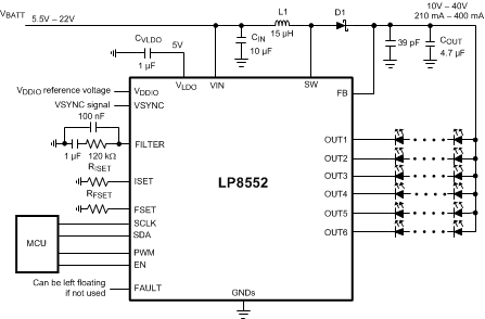 Figure 27. LP8552 with Internal LDO
9.2.1.1 Design Requirements
| DESIGN PARAMETER | EXAMPLE VALUE |
|---|---|
| Input voltage range, VBATT | 5.5 V to 22 V |
| Brightness Control | PWM input duty cycle (default), I2C can be used as well |
| PWM output frequency | With RFSET resistor 85 kΩ to100 kΩ; 9.8 kHz with PSPWM enabled |
| LED Current | With RISET resistor 15 kΩ; 25 mA/channel |
| Brightness slopes | 200-ms linear slope + advanced slope |
| External set resistors | Enabled |
| Inductor | 10 µH to 33 µH, with 2.5-A saturation current |
| Boost SW frequency | 625 kHz |
| SW current limit | 2.5 A |
9.2.1.2 Detailed Design Procedure
9.2.1.2.1 Inductor Selection
There are two main considerations when choosing an inductor; the inductor should not saturate, and the inductor current ripple should be small enough to achieve the desired output voltage ripple. Different saturation current rating specifications are followed by different manufacturers so attention must be given to details. Saturation current ratings are typically specified at 25°C. However, ratings at the maximum ambient temperature of application should be requested from the manufacturer. Shielded inductors radiate less noise and should be preferred.
The saturation current should be greater than the sum of the maximum load current and the worst case average to peak inductor current.
Equation 3 below shows the worst case conditions.
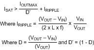
where
- IRIPPLE: Average to peak inductor current
- IOUTMAX: Maximum load current
- VIN: Maximum input voltage in application
- L: Min inductor value including worst case tolerances
- f: Minimum switching frequency
- D: Duty cycle for CCM Operation
- VOUT: Output voltage
Example using Equation 3:
- VIN = 12 V
- VOUT = 38 V
- IOUT = 400 mA
- L = 15 μH − 20% = 12 μH
- f = 1.25 MHz
- ISAT = 1.6 A
As a result the inductor should be selected according to the ISAT. A more conservative and recommended approach is to choose an inductor that has a saturation current rating greater than the maximum current limit of 2.5 A. A 15-μH inductor with a saturation current rating of 2.5 A is recommended for most applications. The inductor’s resistance should be less than 300 mΩ for good efficiency. For high efficiency choose an inductor with high frequency core material such as ferrite to reduce core losses. To minimize radiated noise, use shielded core inductor. Inductor should be placed as close to the SW pin and the IC as possible. Special care should be used when designing the PCB layout to minimize radiated noise and to get good performance from the boost converter.
9.2.1.2.2 Output Capacitor
A ceramic capacitor with 50-V voltage rating or higher is recommended for the output capacitor. The DC-bias effect can reduce the effective capacitance by up to 80%, which needs to be considered in capacitance value selection. For light loads a 4.7-μF capacitor is sufficient. Effectively the capacitance should be 4 μF for < 150 mA loads. For maximum output voltage/current 10-μF capacitor (or two 4.7-μF capacitors) is recommended to minimize the output ripple.
9.2.1.2.3 LDO Capacitor
A 1μF ceramic capacitor with 10-V voltage rating is recommended for the LDO capacitor.
9.2.1.2.4 Output Diode
A Schottky diode should be used for the output diode. Peak repetitive current should be greater than inductor peak current (2.5 A) to ensure reliable operation. Average current rating should be greater than the maximum output current. Schottky diodes with a low forward drop and fast switching speeds are ideal for increasing efficiency in portable applications. Choose a reverse breakdown voltage of the Schottky diode significantly larger (approximately 60 V) than the output voltage. Do not use ordinary rectifier diodes, since slow switching speeds and long recovery times cause the efficiency and the load regulation to suffer.
9.2.1.2.5 Resistors for Setting the LED Current and PWM Frequency
See EEPROM Bit Explanations on how to select values for these resistors.
9.2.1.2.6 Filter Component Values
Optimal components for 60-Hz VSYNC frequency and 4-Hz cut-off frequency of the low-pass filter are shown in Figure 27, Figure 28, Figure 31, and Figure 32. If a 2-Hz cut-off frequency, that is, slower response time is desired, filter components are: C1 = 1 μF, C2 = 10 μF and R = 47 kΩ. If different VSYNC frequency or response time is desired, please contact a TI representative for guidance.
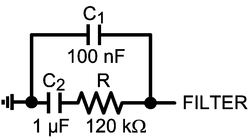 Figure 28. Filter Components
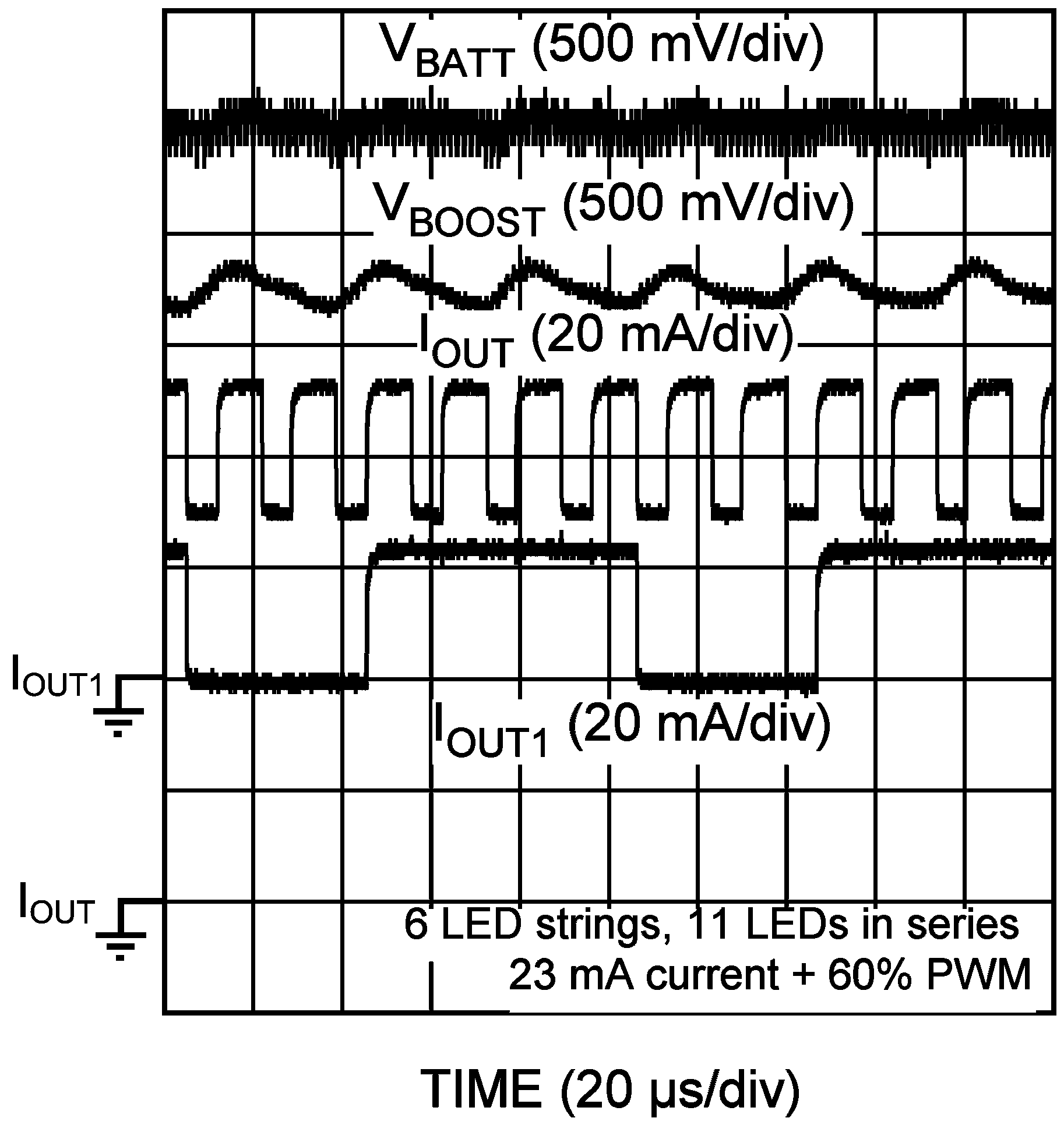
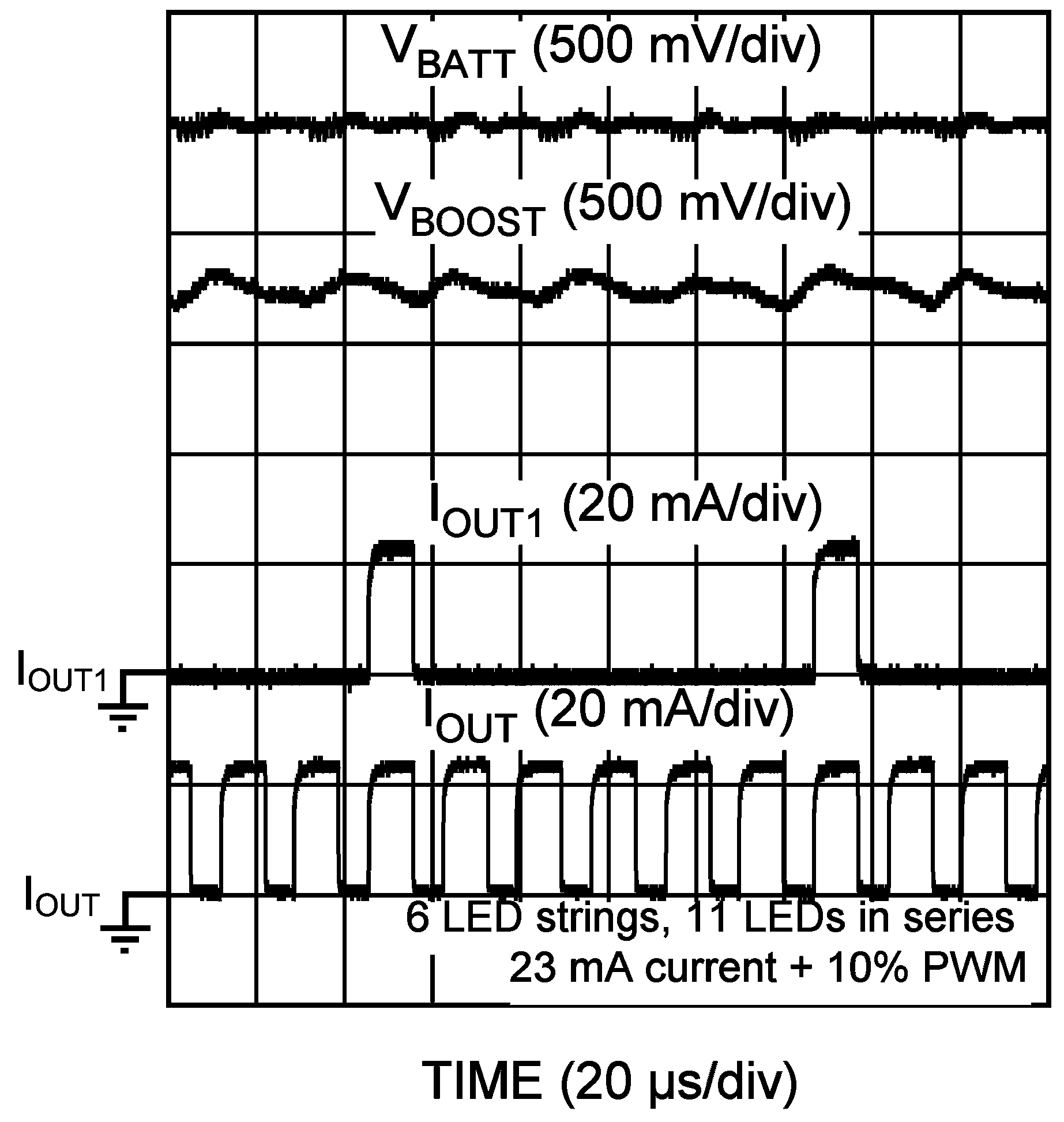
9.2.1.3 Application Curves
Typical Boost and LED Current Waveforms with fLED = 9.6 kHz.
9.2.2 Typical Application for Low Input Voltage
In a single Li-Ion-cell-powered application the internal circuitry of LP8552 can be powered from external 5-V rail. Boost is powered directly from Li-Ion battery and VLDO and VIN pins are connected to external 5-V rail. Current draw from the 5-V rail is maximum 10 mA. A separate 5-V rail to VIN/VLDO can be used also in higher input voltage application to improve efficiency or increase input voltage range above 22 V in some cases. There are no power sequencing requirement for VIN/VLDO and VBATT other than VBATT must be available when enabling backlight to prevent a false overcurrent fault.
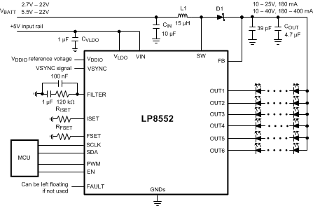 Figure 31. Typical Application for Low Input Voltage
NOTE
Separate 5-V rail to VLDO can be also used to improve efficiency for applications with higher battery voltage. No power sequencing requirements between VIN/VLDO and VBATT.
9.2.2.1 Design Requirements
| DESIGN PARAMETER | EXAMPLE VALUE |
|---|---|
| Input voltage range, VBATT | 2.7 V to VOUT |
| 5-V input rail, VLDO/VIN | 4.5 V to 5.5 V, 10 mA |
| Brightness Control | PWM input duty cycle (default), I2C can be used as well |
| PWM output frequency | With RFSET resistor 85 kΩ to100 kΩ; 9.8 kHz with PSPWM enabled |
| LED Current | With RISET resistor 15 kΩ; 25 mA/channel |
| Brightness slopes | 200-ms linear slope + advanced slope |
| External set resistors | Enabled |
| Inductor | 10 µH to 33 µH, with 2.5-A saturation current |
| Boost SW frequency | 625 kHz |
| SW current limit | 2.5 A |
9.2.2.2 Detailed Design Procedure
Component selection follows Design Requirements above. VLDO capacitor voltage rating can be set based on the 5-V rail voltage specification, which must be < 5.5 V in all cases. Note that UVLO is detected from the VIN pin voltage, not from the VBATT voltage.
9.2.2.3 Application Curves
Typical Boost and LED current behavior is seen in the Application Curves section.
9.2.3 Typical Application for Three Channels and Low Input Voltage
LED outputs can be connected together to be able to drive three channels with possibly higher output current. To maintain the optimum phase shifting OUT1 should be paralleled with OUT4, OUT2 with OUT5, and OUT3 with OUT6.
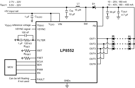 Figure 32. Typical Application For Three Channels and Low Input Voltage
9.2.3.1 Design Requirements
| DESIGN PARAMETER | EXAMPLE VALUE |
|---|---|
| Input voltage range, VBATT | 2.7 V to VOUT |
| 5-V input rail, VLDO/VIN | 4.5 V to 5.5 V, 10 mA |
| Brightness Control | PWM input duty cycle (default), I2C can be used as well |
| PWM output frequency | With RFSET resistor 85 kΩ to100 kΩ; 9.8 kHz with PSPWM enabled |
| LED Current | With RISET resistor 15 kΩ; 50 mA/LED string |
| Brightness slopes | 200-ms linear slope + advanced slope |
| External set resistors | Enabled |
| Inductor | 10 µH to 33 µH, with 2.5-A saturation current |
| Boost SW frequency | 625 kHz |
| SW current limit | 2.5 A |
9.2.3.2 Detailed Design Procedure
Component selection follows Design Requirements above. VLDO capacitor voltage rating can be set based on the 5-V rail voltage specification, which must be < 5.5 V in all cases. Note that UVLO is detected from the VIN pin voltage, not from the VBATT voltage.
9.2.3.3 Application Curves
Typical Boost and LED driver behavior is seen in the Application Curves section.