SNVSBP2 February 2020 LP8758-E3
PRODUCTION DATA.
- 1 Features
- 2 Applications
- 3 Description
- 4 Revision History
- 5 Pin Configuration and Functions
- 6 Specifications
-
7 Detailed Description
- 7.1 Overview
- 7.2 Functional Block Diagram
- 7.3 Feature Description
- 7.4 Device Functional Modes
- 7.5 Programming
- 7.6
Register Maps
- 7.6.1
Register Descriptions
- 7.6.1.1 OTP_REV
- 7.6.1.2 BUCK0_CTRL1
- 7.6.1.3 BUCK0_CTRL2
- 7.6.1.4 BUCK1_CTRL1
- 7.6.1.5 BUCK1_CTRL2
- 7.6.1.6 BUCK2_CTRL1
- 7.6.1.7 BUCK2_CTRL2
- 7.6.1.8 BUCK3_CTRL1
- 7.6.1.9 BUCK3_CTRL2
- 7.6.1.10 BUCK0_VOUT
- 7.6.1.11 BUCK0_FLOOR_VOUT
- 7.6.1.12 BUCK1_VOUT
- 7.6.1.13 BUCK1_FLOOR_VOUT
- 7.6.1.14 BUCK2_VOUT
- 7.6.1.15 BUCK2_FLOOR_VOUT
- 7.6.1.16 BUCK3_VOUT
- 7.6.1.17 BUCK3_FLOOR_VOUT
- 7.6.1.18 BUCK0_DELAY
- 7.6.1.19 BUCK1_DELAY
- 7.6.1.20 BUCK2_DELAY
- 7.6.1.21 BUCK3_DELAY
- 7.6.1.22 RESET
- 7.6.1.23 CONFIG
- 7.6.1.24 INT_TOP
- 7.6.1.25 INT_BUCK_0_1
- 7.6.1.26 INT_BUCK_2_3
- 7.6.1.27 TOP_STAT
- 7.6.1.28 BUCK_0_1_STAT
- 7.6.1.29 BUCK_2_3_STAT
- 7.6.1.30 TOP_MASK
- 7.6.1.31 BUCK_0_1_MASK
- 7.6.1.32 BUCK_2_3_MASK
- 7.6.1.33 SEL_I_LOAD
- 7.6.1.34 I_LOAD_2
- 7.6.1.35 I_LOAD_1
- 7.6.1
Register Descriptions
- 8 Application and Implementation
- 9 Power Supply Recommendations
- 10Layout
- 11Device and Documentation Support
- 12Mechanical, Packaging, and Orderable Information
Package Options
Mechanical Data (Package|Pins)
- YFF|35
Thermal pad, mechanical data (Package|Pins)
Orderable Information
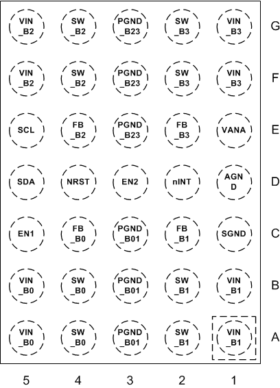
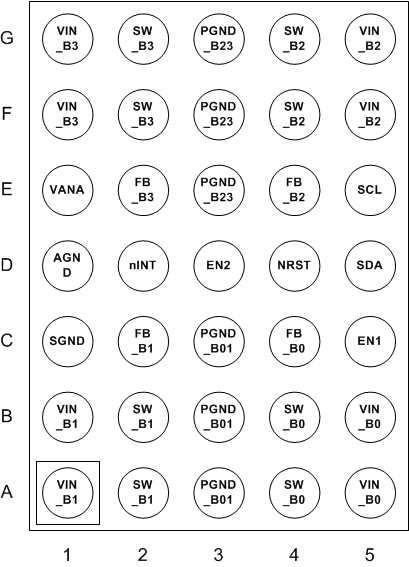
5 Pin Configuration and Functions
YFF Package
35-Pin DSBGA
Top View

YFF Package
35-Pin DSBGA
Bottom View

Pin Functions
| PIN | TYPE | DESCRIPTION | |
|---|---|---|---|
| NUMBER | NAME | ||
| A1, B1 | VIN_B1 | P | Input for Buck1. The separate power pins VIN_Bx are not connected together internally – VIN_Bx pins must be connected together in the application and be locally bypassed. |
| A2, B2 | SW_B1 | A | Buck1 switch node. |
| A3, B3, C3 | PGND_B01 | G | Power Ground for Buck0 and Buck1. |
| A4, B4 | SW_B0 | A | Buck0 switch node. |
| A5, B5 | VIN_B0 | P | Input for Buck0. The separate power pins VIN_Bx are not connected together internally – VIN_Bx pins must be connected together in the application and be locally bypassed. |
| C1 | SGND | G | Substrate Ground. |
| C2 | FB_B1 | A | Output voltage feedback for Buck1. |
| C4 | FB_B0 | A | Output voltage feedback for Buck0. |
| C5 | EN1 | D/I | Programmable Enable signal for Buck converter core or cores. Can be also configured to switch between two output voltage levels. |
| D1 | AGND | G | Ground. |
| D2 | nINT | D/O | Open-drain interrupt output. Active LOW. |
| D3 | EN2 | D/I | Programmable Enable signal for Buck converter one or more cores. Can be also configured to switch between two output voltage levels. |
| D4 | NRST | D/I | Reset signal for the device. Can be also used to enable the regulator. |
| D5 | SDA | D/I/O | Serial interface data input and output for system access. Connect a pullup resistor. |
| E1 | VANA | P | Supply voltage for Analog and Digital blocks. |
| E2 | FB_B3 | A | Output voltage feedback for Buck3. |
| E4 | FB_B2 | A | Output voltage feedback for Buck2. |
| E5 | SCL | D/I | Serial interface clock input for system access. Connect a pullup resistor. |
| F1, G1 | VIN_B3 | P | Input for Buck3. The separate power pins VIN_Bx are not connected together internally – VIN_Bx pins must be connected together in the application and be locally bypassed. |
| F2, G2 | SW_B3 | A | Buck3 switch node. |
| E3, F3, G3 | PGND_B23 | G | Power Ground for Buck2 and Buck3. |
| F4, G4 | SW_B2 | A | Buck2 switch node. |
| F5, G5 | VIN_B2 | P | Input for Buck2. The separate power pins VIN_Bx are not connected together internally - VIN_Bx pins must be connected together in the application and be locally bypassed. |
| A: Analog Pin, D: Digital Pin, G: Ground Pin, P: Power Pin, I: Input Pin, O: Output Pin | |||