SDLS972B April 2023 – April 2024 LSF0102
PRODUCTION DATA
- 1
- 1 Features
- 2 Applications
- 3 Description
- 4 Pin Configuration and Functions
-
5 Specifications
- 5.1 Absolute Maximum Ratings
- 5.2 ESD Ratings
- 5.3 Recommended Operating Conditions
- 5.4 Thermal Information
- 5.5 Electrical Characteristics
- 5.6 LSF0102 AC Performance (Translating Down) Switching Characteristics , VCCB = 3.3V
- 5.7 LSF0102 AC Performance (Translating Down) Switching Characteristics, VCCB = 2.5V
- 5.8 LSF0102 AC Performance (Translating Up) Switching Characteristics, VCCB = 3.3V
- 5.9 LSF0102 AC Performance (Translating Up) Switching Characteristics, VCCB = 2.5V
- 5.10 Typical Characteristics
- 6 Parameter Measurement Information
- 7 Detailed Description
- 8 Application and Implementation
- 9 Device and Documentation Support
- 10Mechanical, Packaging, and Orderable Information
- 11Revision History
Package Options
Refer to the PDF data sheet for device specific package drawings
Mechanical Data (Package|Pins)
- DCU|8
- DDF|8
- DTM|8
- YZT|8
- DCT|8
- DQE|8
Thermal pad, mechanical data (Package|Pins)
Orderable Information
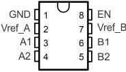
4 Pin Configuration and Functions
Pinout drawings are not to scale
Pinout drawings are not to scale Figure 4-1 LSF0102 DCT, DCU or DDF Package,
8-Pin SM8, VSSOP, or SOT-23
(Top View). Pinout drawings are not to scale
 Figure 4-1 LSF0102 DCT, DCU or DDF Package,
8-Pin SM8, VSSOP, or SOT-23
(Top View). Pinout drawings are not to scale
Figure 4-1 LSF0102 DCT, DCU or DDF Package,
8-Pin SM8, VSSOP, or SOT-23
(Top View). Pinout drawings are not to scalePinout drawings are not to scale Figure 4-3 LSF0102 DTM Package,
8-Pin X2SON
(Transparent Top View). Pinout drawings are not to scale
 Figure 4-3 LSF0102 DTM Package,
8-Pin X2SON
(Transparent Top View). Pinout drawings are not to scale
Figure 4-3 LSF0102 DTM Package,
8-Pin X2SON
(Transparent Top View). Pinout drawings are not to scalePinout drawings are not to scale Figure 4-2 LSF0102 DQE Package,
8-Pin X2SON
(Transparent Top View). Pinout drawings are not to scale
 Figure 4-2 LSF0102 DQE Package,
8-Pin X2SON
(Transparent Top View). Pinout drawings are not to scale
Figure 4-2 LSF0102 DQE Package,
8-Pin X2SON
(Transparent Top View). Pinout drawings are not to scaleTable 4-1 Pin Functions
| PIN | TYPE(1) | DESCRIPTION | |
|---|---|---|---|
| NAME | NO. | ||
| An | 3, 4 | I/O | Auto-Bidirectional Data port |
| Bn | 6, 5 | I/O | |
| EN | 8 | I | Enable input; connect to Vref_B and pull-up through a high resistor (200kΩ). See Using the Enable Pin with the LSF Family |
| GND | 1 | — | Ground |
| Vref_A | 2 | — | Reference supply
voltage. For proper device biasing, see Section 8 and Understanding the Bias Circuit for the LSF Family. |
| Vref_B | 7 | — | |
(1) I= input, O = output
 Figure 4-4 LSF0102 YZT Package,
8-Pin DSBGA
(Bottom View)
Figure 4-4 LSF0102 YZT Package,
8-Pin DSBGA
(Bottom View)| Legend | |
|---|---|
| Input | Input or Output |
| Ground | |
Table 4-2 Pin Functions
| PIN | TYPE(1) | DESCRIPTION | |
|---|---|---|---|
| NO. | NAME | ||
| C1 | A1 | I/O | Auto-Bidirectional Data port |
| D1 | A2 | I/O | |
| C2 | B1 | I/O | |
| D2 | B2 | I/O | |
| B1 | Vref_A | — | Reference supply voltage. For proper device biasing, see Section 8 and Understanding the Bias Circuit for the LSF Family. |
| B2 | Vref_B | — | |
| A2 | EN | I | Enable input; connect to Vref_B and pull-up through a high resistor (200kΩ). See Using the Enable Pin with the LSF Family |
| A1 | GND | — | Ground |
(1) I= input, O = output