SLVS033G February 1990 – July 2015 LT1054
PRODUCTION DATA.
- 1 Features
- 2 Applications
- 3 Description
- 4 Revision History
- 5 Pin Configuration and Functions
- 6 Specifications
- 7 Detailed Description
- 8 Application and Implementation
- 9 Power Supply Recommendations
- 10Layout
- 11Device and Documentation Support
- 12Mechanical, Packaging, and Orderable Information
Package Options
Refer to the PDF data sheet for device specific package drawings
Mechanical Data (Package|Pins)
- P|8
- DW|16
Thermal pad, mechanical data (Package|Pins)
- DW|16
Orderable Information
5 Pin Configuration and Functions
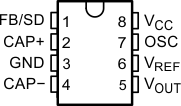
P Package
8-Pin PDIP
Top View

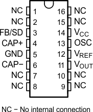
DW Package
16-Pin SOIC
Top View

Pin Functions
| PIN | I/O | DESCRIPTION | ||
|---|---|---|---|---|
| NAME | PDIP | SOIC | ||
| FB/SD | 1 | 3 | Input | Shutdown for low Iq operation or error amp input for regulation |
| CAP+ | 2 | 4 | Input | Positive side of CIN |
| GND | 3 | 5 | — | Ground |
| CAP- | 4 | 6 | Input | Negative side of CIN |
| VOUT | 5 | 11 | Output | Regulated output voltage |
| VREF | 6 | 12 | Output | Internal Reference Voltage |
| OSC | 7 | 13 | Input | Oscillator control pin |
| VCC | 8 | 14 | — | Supply pin |
| NC | — | 1, 2, 7, 8, 9, 10, 15, 16 | — | No connect (no internal connection) |