SLVS033G February 1990 – July 2015 LT1054
PRODUCTION DATA.
- 1 Features
- 2 Applications
- 3 Description
- 4 Revision History
- 5 Pin Configuration and Functions
- 6 Specifications
- 7 Detailed Description
- 8 Application and Implementation
- 9 Power Supply Recommendations
- 10Layout
- 11Device and Documentation Support
- 12Mechanical, Packaging, and Orderable Information
Package Options
Refer to the PDF data sheet for device specific package drawings
Mechanical Data (Package|Pins)
- P|8
- DW|16
Thermal pad, mechanical data (Package|Pins)
- DW|16
Orderable Information
6 Specifications
6.1 Absolute Maximum Ratings
over operating free-air temperature range (unless otherwise noted)(1)| MIN | MAX | UNIT | ||||
|---|---|---|---|---|---|---|
| VCC | Supply voltage(2) | 16 | V | |||
| VI | Input voltage | FB/SD | 0 | VCC | V | |
| OSC | 0 | Vref | V | |||
| TJ | Junction temperature(3) | LT1054C | 125 | °C | ||
| LT1054I | 135 | °C | ||||
| Tstg | Storage temperature | –55 | 150 | °C | ||
(1) Stresses beyond those listed under Absolute Maximum Ratings may cause permanent damage to the device. These are stress ratings only, which do not imply functional operation of the device at these or any other conditions beyond those indicated under Recommended Operating Conditions. Exposure to absolute-maximum-rated conditions for extended periods may affect device reliability.
(2) The absolute maximum supply-voltage rating of 16 V is for unregulated circuits. For regulation-mode circuits with VOUT ≤ 15 V, this rating may be increased to 20 V.
(3) The devices are functional up to the absolute maximum junction temperature.
6.2 ESD Ratings
| VALUE | UNIT | |||
|---|---|---|---|---|
| V(ESD) | Electrostatic discharge | Human body model (HBM), per ANSI/ESDA/JEDEC JS-001(1) | ±500 | V |
| Charged-device model (CDM), per JEDEC specification JESD22-C101(2) | ±3500 | |||
(1) JEDEC document JEP155 states that 500-V HBM allows safe manufacturing with a standard ESD control process.
(2) JEDEC document JEP157 states that 250-V CDM allows safe manufacturing with a standard ESD control process.
6.3 Recommended Operating Conditions
over operating free-air temperature range (unless otherwise noted)| MIN | MAX | UNIT | |||
|---|---|---|---|---|---|
| VCC | Supply voltage | 3.5 | 15 | V | |
| TA | Operating free-air temperature range | LT1054C | 0 | 70 | °C |
| LT1054I | –40 | 85 | |||
6.4 Thermal Information
| THERMAL METRIC(1) | LT1054 | UNIT | ||
|---|---|---|---|---|
| P (PDIP) | DW (SOIC) | |||
| 8 PINS | 16 PINS | |||
| RθJA | Junction-to-ambient thermal resistance | 85 | 57 | °C/W |
(1) For more information about traditional and new thermal metrics, see the Semiconductor and IC Package Thermal Metrics application report, SPRA953.
6.5 Electrical Characteristics
over recommended operating free-air temperature range (unless otherwise noted)| PARAMETER | TEST CONDITIONS | TA(1) | LT1054C, LT1054I | UNIT | ||||
|---|---|---|---|---|---|---|---|---|
| MIN | TYP(2) | MAX | ||||||
| VO | Regulated output voltage | VCC = 7 V, TJ = 25°C, RL = 500 Ω (3) | 25°C | −4.7 | −5 | −5.2 | V | |
| Input regulation | VCC = 7 V to 12 V, RL = 500 Ω(3) | Full range | 5 | 25 | mV | |||
| Output regulation | VCC = 7 V, RL = 100 Ω to 500 Ω(3) | Full range | 10 | 50 | mV | |||
| Voltage loss, VCC − |VO| (4) |
CI = CO = 100-μF tantalum | IO = 10 mA | Full range | 0.35 | 0.55 | V | ||
| IO = 100 mA | 1.1 | 1.6 | ||||||
| Output resistance | ΔIO = 10 mA to 100 mA | See (5) | Full range | 10 | 15 | Ω | ||
| Oscillator frequency | VCC = 3.5 V to 15 V | Full range | 15 | 25 | 35 | kHz | ||
| Vref | Reference voltage | I(REF) = 60 μA | 25°C | 2.35 | 2.5 | 2.65 | V | |
| Full range | 2.25 | 2.75 | ||||||
| Maximum switch current | 25°C | 300 | 4 | mA | ||||
| ICC | Supply current | IO = 0 | VCC = 3.5 V | Full range | 2.5 | 5 | mA | |
| VCC = 15 V | 3 | 200 | ||||||
| Supply current in shutdown | V(FB/SD) = 0 V | Full range | 100 | μA | ||||
(1) Full range is 0°C to 70°C for the LT1054C and −40°C to 85°C for the LT1054I.
(2) All typical values are at TA = 25°C.
(3) All regulation specifications are for a device connected as a positive-to-negative converter/regulator with R1 = 20 kΩ, R2 = 102.5 kΩ, external capacitor CIN = 10 μF (tantalum), external capacitor COUT = 100 μF (tantalum) and C1 = 0.002 μF (see ).
(4) For voltage-loss tests, the device is connected as a voltage inverter, with terminals 1, 6, and 7 unconnected. The voltage losses may be higher in other configurations. CIN and COUT are external capacitors.
(5) Output resistance is defined as the slope of the curve (ΔVO versus ΔIO) for output currents of 10 mA to 100 mA. This represents the linear portion of the curve. The incremental slope of the curve is higher at currents less than 10 mA due to the characteristics of the switch transistors.
6.6 Typical Characteristics
Data at high and low temperatures are applicable only within the recommended operating free-air temperature range.Table 1. Table of Graphs
| FIGURE | ||
|---|---|---|
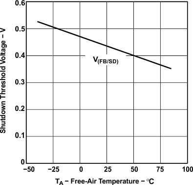
| Shutdown threshold voltage | vs Free-air temperature | Figure 1 |
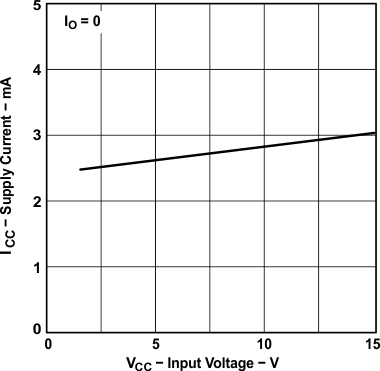
| Supply current | vs Input voltage | Figure 2 |
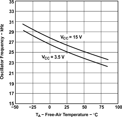
| Oscillator frequency | vs Free-air temperature | Figure 3 |
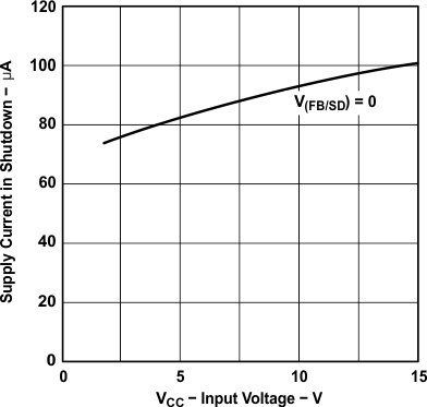
| Supply current in shutdown | vs Input voltage | Figure 4 |
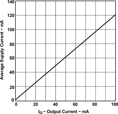
| Average supply current | vs Output current | Figure 5 |
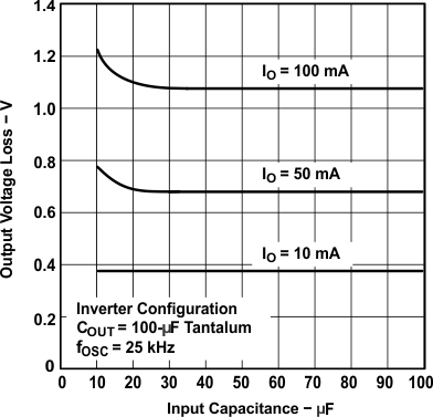
| Output voltage loss | vs Input capacitance | Figure 6 |
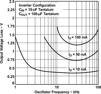
| Output voltage loss | vs Oscillator frequency (10 µF) | Figure 7 |
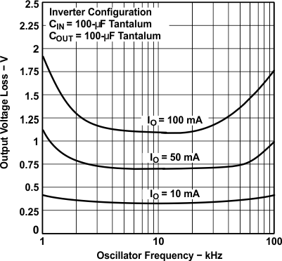
| Output voltage loss | vs Oscillator frequency (100 µF) | Figure 8 |
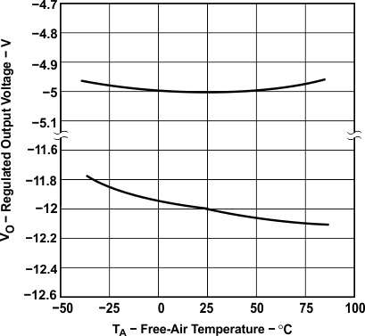
| Regulated output voltage | vs Free-air temperature | Figure 9 |
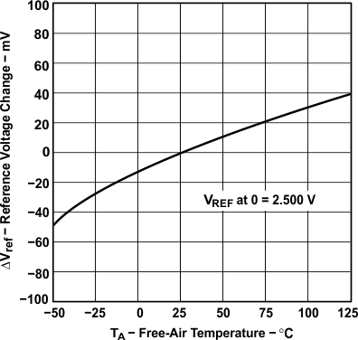
| Reference voltage change | vs Free-air temperature | Figure 10 |
| Voltage loss | vs Output current | Figure 17 |
