SLLS664E August 2005 – June 2021 MAX3232E
PRODUCTION DATA
- 1 Features
- 2 Applications
- 3 Description
- 4 Revision History
- 5 Pin Configuration and Functions
-
6 Specifications
- 6.1 Absolute Maximum Ratings
- 6.2 ESD Ratings
- 6.3 ESD Ratings - IEC Specifications
- 6.4 Recommended Operating Conditions (1)
- 6.5 Thermal Information
- 6.6 Electrical Characteristics — Device (1)
- 6.7 Electrical Characteristics — Driver (1)
- 6.8 Electrical Characteristics — Receiver (1)
- 6.9 Switching Characteristics (1)
- 6.10 Typical Characteristics
- 7 Parameter Measurement Information
- 8 Detailed Description
- 9 Application and Implementation
- 10Power Supply Recommendations
- 11Layout
- 12Device and Documentation Support
Package Options
Mechanical Data (Package|Pins)
Thermal pad, mechanical data (Package|Pins)
- DW|16
Orderable Information
5 Pin Configuration and Functions
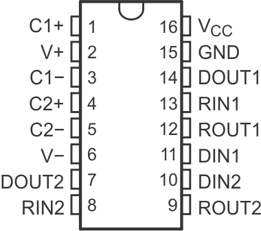
 Figure 5-1 D, DW, DB and PW Package,
16-Pin SOIC, SSOP and TSSOP, Top View
Figure 5-1 D, DW, DB and PW Package,
16-Pin SOIC, SSOP and TSSOP, Top ViewTable 5-1 Pin Functions
| PIN | I/O | DESCRIPTION | |
|---|---|---|---|
| NAME | NO. | ||
| C1+ | 1 | — | Positive lead of C1 capacitor |
| V+ | 2 | O | Positive charge pump output for storage capacitor only |
| C1– | 3 | — | Negative lead of C1 capacitor |
| C2+ | 4 | — | Positive lead of C2 capacitor |
| C2– | 5 | — | Negative lead of C2 capacitor |
| V– | 6 | O | Negative charge pump output for storage capacitor only |
| DOUT2 | 7 | O | RS232 line data output (to remote RS232 system) |
| RIN2 | 8 | I | RS232 line data input (from remote RS232 system) |
| ROUT2 | 9 | O | Logic data output (to UART) |
| DIN2 | 10 | I | Logic data input (from UART) |
| DIN1 | 11 | I | Logic data input (from UART) |
| ROUT1 | 12 | O | Logic data output (to UART) |
| RIN1 | 13 | I | RS232 line data input (from remote RS232 system) |
| DOUT1 | 14 | O | RS232 line data output (to remote RS232 system) |
| GND | 15 | — | Ground |
| VCC | 16 | — | Supply Voltage, Connect to external 3-V to 5.5-V power supply |