SLAS697E March 2010 – November 2016 MSP430F2619S-HT
PRODUCTION DATA.
- 1Device Overview
- 2Revision History
- 3Terminal Configurations and Functions
-
4Specifications
- 4.1 Absolute Maximum Ratings
- 4.2 ESD Ratings
- 4.3 Recommended Operating Conditions
- 4.4 Thermal Information
- 4.5 Active-Mode Supply Current Into AVCC Excluding External Current - Electrical Characteristics
- 4.6 Typical Characteristics - Active-Mode Supply Current (Into DVCC + AVCC)
- 4.7 Active-Mode Current vs DCO Frequency
- 4.8 Low-Power-Mode Supply Currents Into AVCC Excluding External Current - Electrical Characteristics
- 4.9 Typical Characteristics - LPM4 Current
- 4.10 Schmitt-Trigger Inputs (Ports P1 Through P6, and RST/NMI, JTAG, XIN, and XT2IN) - Electrical Characteristics
- 4.11 Inputs (Ports P1 and P2) - Electrical Characteristics
- 4.12 Leakage Current (Ports P1 Through P6) - Electrical Characteristics
- 4.13 Standard Inputs - RST/NMI - Electrical Characteristics
- 4.14 Outputs (Ports P1 Through P6) - Electrical Characteristics
- 4.15 Output Frequency (Ports P1 Through P6) - Electrical Characteristics
- 4.16 Typical Characteristics - Outputs
- 4.17 POR/Brownout Reset (BOR) - Electrical Characteristics
- 4.18 Typical Characteristics - POR/Brownout Reset (BOR)
- 4.19 SVS (Supply Voltage Supervisor/Monitor) - Electrical Characteristics
- 4.20 Typical Characteristics - SVS
- 4.21 Main DCO Characteristics
- 4.22 DCO Frequency - Electrical Characteristics
- 4.23 Calibrated DCO Frequencies (Tolerance at Calibration) - Electrical Characteristics
- 4.24 Calibrated DCO Frequencies (Tolerance Over Temperature) - Electrical Characteristics
- 4.25 Calibrated DCO Frequencies (Tolerance Over Supply Voltage VCC) - Electrical Characteristics
- 4.26 Calibrated DCO Frequencies (Overall Tolerance) - Electrical Characteristics
- 4.27 Typical Characteristics - Calibrated DCO Frequency
- 4.28 Wake-Up From Low-Power Modes (LPM3/4) - Electrical Characteristics
- 4.29 Typical Characteristics - DCO Clock Wake-Up Time From LPM3/4
- 4.30 DCO With External Resistor ROSC - Electrical Characteristics
- 4.31 Typical Characteristics - DCO With External Resistor ROSC
- 4.32 Crystal Oscillator (LFXT1) Low-Frequency Modes - Electrical Characteristics
- 4.33 Internal Very-Low-Power, Low-Frequency Oscillator (VLO) - Electrical Characteristics
- 4.34 Crystal Oscillator (LFXT1) High Frequency Modes - Electrical Characteristics
- 4.35 Typical Characteristics - LFXT1 Oscillator in HF Mode (XTS = 1)
- 4.36 Crystal Oscillator (XT2) - Electrical Characteristics
- 4.37 Typical Characteristics - XT2 Oscillator
- 4.38 Timer_A - Electrical Characteristics
- 4.39 Timer_B - Electrical Characteristics
- 4.40 USCI (UART Mode) - Electrical Characteristics
- 4.41 USCI (SPI Master Mode) - Electrical Characteristics
- 4.42 USCI (SPI Slave Mode) - Electrical Characteristics
- 4.43 USCI (I2C Mode) - Electrical Characteristics
- 4.44 Comparator_A+ - Electrical Characteristics
- 4.45 Typical Characteristics - Comparator A+
- 4.46 12-Bit ADC Power-Supply and Input Range Conditions - Electrical Characteristics
- 4.47 12-Bit ADC External Reference - Electrical Characteristics
- 4.48 12-Bit ADC Built-In Reference - Electrical Characteristics
- 4.49 Typical Characteristics - ADC12
- 4.50 12-Bit ADC Timing Parameters - Electrical Characteristics
- 4.51 12-Bit ADC Linearity Parameters - Electrical Characteristics
- 4.52 12-Bit ADC Temperature Sensor and Built-In VMID - Electrical Characteristics
- 4.53 12-Bit DAC Supply Specifications - Electrical Characteristics
- 4.54 12-Bit DAC Linearity Parameters - Electrical Characteristics
- 4.55 Typical Characteristics - 12-Bit DAC Linearity Specifications
- 4.56 12-Bit DAC Output Specifications - Electrical Characteristics
- 4.57 12-Bit DAC Reference Input Specifications - Electrical Characteristics
- 4.58 12-Bit DAC Dynamic Specifications, VREF = VCC, DAC12IR = 1 - Electrical Characteristics
- 4.59 Flash Memory - Electrical Characteristics
- 4.60 RAM - Electrical Characteristics
- 4.61 JTAG and Spy-Bi-Wire Interface - Electrical Characteristics
- 4.62 JTAG Fuse - Electrical Characteristics
-
5Detailed Description
- 5.1 CPU
- 5.2 Instruction Set
- 5.3 Operating Modes
- 5.4 Interrupt Vector Addresses
- 5.5 Special Function Registers
- 5.6 Memory Organization
- 5.7 Bootstrap Loader (BSL)
- 5.8 Flash Memory
- 5.9 Peripherals
- 5.10 DMA Controller
- 5.11 Oscillator and System Clock
- 5.12 Brownout, Supply Voltage Supervisor (SVS)
- 5.13 Digital I/O
- 5.14 WDT+ Watchdog Timer
- 5.15 Hardware Multiplier
- 5.16 USCI
- 5.17 Timer_A3
- 5.18 Timer_B7
- 5.19 Comparator_A+
- 5.20 ADC12
- 5.21 DAC12
- 5.22 Peripheral File Map
-
6Applications, Implementation, and Layout
- 6.1 P1.0 to P1.7, Input/Output With Schmitt Trigger
- 6.2 P2.0 to P2.4, P2.6, and P2.7, Input/Output With Schmitt Trigger
- 6.3 P2.5, Input/Output With Schmitt Trigger and External ROSC for DCO
- 6.4 Port P3 Pin Schematic: P3.0 to P3.7, Input/Output With Schmitt Trigger
- 6.5 Port P4 Pin Schematic: P4.0 to P4.7, Input/Output With Schmitt Trigger
- 6.6 Port P5 Pin Schematic: P5.0 to P5.7, Input/Output With Schmitt Trigger
- 6.7 Port P6 Pin Schematic: P6.0 to P6.4, Input/Output With Schmitt Trigger
- 6.8 Port P6 Pin Schematic: P6.5 and P6.6, Input/Output With Schmitt Trigger
- 6.9 Port P6 Pin Schematic: P6.7, Input/Output With Schmitt Trigger
- 6.10 Port P7 Pin Schematic: P7.0 to P7.7, Input/Output With Schmitt Trigger
- 6.11 Port P8 Pin Schematic: P8.0 to P8.5, Input/Output With Schmitt Trigger
- 6.12 Port P8 Pin Schematic: P8.6, Input/Output With Schmitt Trigger
- 6.13 Port P8 Pin Schematic: P8.7, Input/Output With Schmitt Trigger
- 6.14 JTAG Pins: TMS, TCK, TDI/TCLK, TDO/TDI, Input/Output With Schmitt Trigger
- 6.15 JTAG Fuse Check Mode
- 7Device and Documentation Support
- 8Mechanical, Packaging, and Orderable Information
Package Options
Mechanical Data (Package|Pins)
- PM|64
- KGD|0
Thermal pad, mechanical data (Package|Pins)
Orderable Information
6 Applications, Implementation, and Layout
6.1 P1.0 to P1.7, Input/Output With Schmitt Trigger
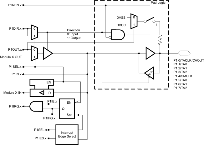 Figure 6-1 Port P1 (P1.0 to P1.7) Pin Schematic
Table 6-1 Port P1 (P1.0 to P1.7) Pin Functions
| PIN NAME (P1.X) | X | FUNCTION | CONTROL BITS/SIGNALS | |
|---|---|---|---|---|
| P1DIR.x | P1SEL.x | |||
| P1.0/TACLK/ADC10CLK | 0 | P1.0 | I: 0; O: 1 | 0 |
| Timer_A3.TACLK | 0 | 1 | ||
| ADC10CLK | 1 | 1 | ||
| P1.1/TA0 | 1 | P1.1 (I/O) | I: 0; O: 1 | 0 |
| Timer_A3.CCI0A | 0 | 1 | ||
| Timer_A3.TA0 | 1 | 1 | ||
| P1.2/TA1 | 2 | P1.2 (I/O) | I: 0; O: 1 | 0 |
| Timer_A3.CCI0A | 0 | 1 | ||
| Timer_A3.TA0 | 1 | 1 | ||
| P1.3/TA2 | 3 | P1.3 I/O | I: 0; O: 1 | 0 |
| Timer_A3.CCI0A | 0 | 1 | ||
| Timer_A3.TA0 | 1 | 1 | ||
| P1.4/SMCLK | 4 | P1.4 (I/O) | I: 0; O: 1 | 0 |
| SMCLK | 1 | 1 | ||
| P1.5/TA0 | 5 | P1.5 (I/O) | I: 0; O: 1 | 0 |
| Timer_A3.TA0 | 1 | 1 | ||
| P1.6/TA1 | 6 | P1.6 (I/O) | I: 0; O: 1 | 0 |
| Timer_A3.TA1 | 1 | 1 | ||
| P1.7/TA2 | 7 | P1.7 (I/O) | I: 0; O: 1 | 0 |
| Timer_A3.TA2 | 1 | 1 | ||
6.2 P2.0 to P2.4, P2.6, and P2.7, Input/Output With Schmitt Trigger
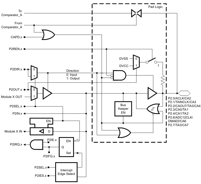 Figure 6-2 Port P2.0, P2.3, P2.4, P2.6 and P2.7 Pin Schematic
Table 6-2 Port P2.0, P2.3, P2.4, P2.6 and P2.7 Pin Functions
| Pin Name (P2.X) | X | FUNCTION | CONTROL BITS/SIGNALS(1) | ||
|---|---|---|---|---|---|
| CAPD.x | P2DIR.x | P2SEL.x | |||
| P2.0/ACLK/CA2 | 0 | P2.0 (I/O) | 0 | I: 0; O: 1 | 0 |
| ACLK | 0 | 1 | 1 | ||
| CA2 | 1 | X | X | ||
| P2.1/TAINCLK/CA3 | 1 | P2.2 (I/O) | 0 | I: 0; O: 1 | 0 |
| Timer_A3.INCLK | 0 | 0 | 1 | ||
| DVSS | 0 | 1 | 1 | ||
| CA3 | 1 | X | X | ||
| P2.2/CAOUT/TA0/CA4 | 2 | P2.2 (I/O) | 0 | I: 0; O: 1 | 0 |
| CAOUT | 0 | 1 | 1 | ||
| Timer_A3.CCI0B | 0 | 0 | 1 | ||
| CA4 | 1 | X | X | ||
| P2.3/CA0/TA1 | 3 | P2.3 (I/O) | 0 | I: 0; O: 1 | 0 |
| Timer_A3.TA1 | 0 | 1 | 1 | ||
| CA0 | 1 | X | X | ||
| P2.4/CA1/TA2 | 4 | P2.4 (I/O) | 0 | I: 0; O: 1 | 0 |
| Timer_A3.TA2 | 0 | 1 | X | ||
| CA1 | 1 | X | 1 | ||
| P2.6/ADC12CLK/ DMAE0/CA6 |
6 | P2.6 (I/O) | 0 | I: 0; O: 1 | 0 |
| ADC12CLK | 0 | 1 | 1 | ||
| DMAE0 | 0 | 0 | 1 | ||
| CA6 | 1 | X | X | ||
| P2.7/TA0/CA7 | 7 | P2.7 (I/O) | 0 | I: 0; O: 1 | 0 |
| Timer_A3.TA0 | 0 | 1 | 1 | ||
| CA7 | 1 | X | X | ||
6.3 P2.5, Input/Output With Schmitt Trigger and External ROSC for DCO
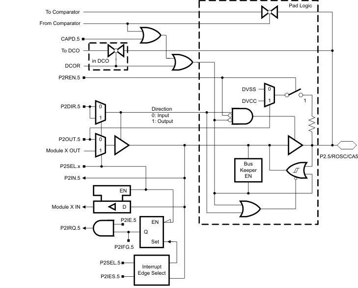 Figure 6-3 Port P2 (P2.5) Pin Schematic
6.4 Port P3 Pin Schematic: P3.0 to P3.7, Input/Output With Schmitt Trigger
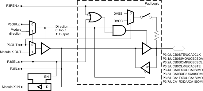 Figure 6-4 Port P3 (P3.0) Pin Schematic
Table 6-4 Port P3 (P3.0) Pin Functions
| PIN NAME (P3.X) | X | FUNCTION | CONTROL BITS/SIGNALS(1) | |
|---|---|---|---|---|
| P3DIR.x | P3SEL.x | |||
| P3.0/UCB0STE/UCA0CLK | 0 | P3.0 (I/O) | I: 0; O: 1 | 0 |
| UCB0STE/UCA0CLK(2)(3) | X | 1 | ||
| P3.1/UCB0SIMO/UCB0SDA | 1 | P3.1 (I/O) | I: 0; O: 1 | 0 |
| UCB0SIMO/UCB0SDA(2)(4) | X | 1 | ||
| P3.2/UCB0SOMI/UCB0SCL | 2 | P3.2 (I/O | I: 0; O: 1 | 0 |
| UCB0SOMI/UCB0SCL(2)(4) | X | 1 | ||
| P3.3/UCB0CLK/UCA0STE | 3 | P3.3 (I/O) | I: 0; O: 1 | 0 |
| UCB0CLK/UCA0STE(2) | X | 1 | ||
| P3.4/UCA0TXD/UCA0SIMO | 4 | P3.4 (I/O) | I: 0; O: 1 | 0 |
| UCA0TXD/UCA0SIMO(2) | X | 1 | ||
| P3.5/UCA0RXD/UCA0SOMI | 5 | P3.5 (I/O) | I: 0; O: 1 | 0 |
| UCA0RXD/UCA0SOMI(2) | X | 1 | ||
| P3.6/UCA1TXD/UCA1SIMO | 6 | P3.6 (I/O) | I: 0; O: 1 | 0 |
| UCA1TXD/UCA1SIMO(2) | X | 1 | ||
| P3.7/UCA1RXD/UCA1SOMI | 7 | P3.7 (I/O) | I: 0; O: 1 | 0 |
| UCA1RXD/UCA1SOMI(2) | X | 1 | ||
6.5 Port P4 Pin Schematic: P4.0 to P4.7, Input/Output With Schmitt Trigger
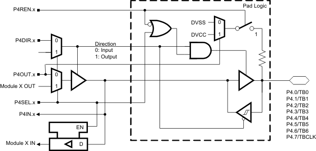 Figure 6-5 Port P4 (P4.0 to P4.7) Pin Schematic
Table 6-5 Port P4 (P4.0 to P4.7) Pin Functions
| PIN NAME (P4.X) | X | FUNCTION | CONTROL BITS/SIGNALS | |
|---|---|---|---|---|
| P4DIR.x | P4SEL.x | |||
| P4.0/TB0 | 0 | P4.0 (I/O) | I: 0; O: 1 | 0 |
| Timer_B7.CCI0A and Timer_B7.CCI0B | 0 | 1 | ||
| Timer_B7.TB0 | 1 | 1 | ||
| P4.1/TB1 | 1 | P4.1 (I/O) | I: 0; O: 1 | 0 |
| Timer_B7.CCI1A and Timer_B7.CCI1B | 0 | 1 | ||
| Timer_B7.TB1 | 1 | 1 | ||
| P4.2/TB2 | 2 | P4.2 (I/O) | I: 0; O: 1 | 0 |
| Timer_B7.CCI2A and Timer_B7.CCI2B | 0 | 1 | ||
| Timer_B7.TB2 | 1 | 1 | ||
| P4.3/TB3 | 3 | P4.3 (I/O) | I: 0; O: 1 | 0 |
| Timer_B7.CCI3A and Timer_B7.CCI3B | 0 | 1 | ||
| Timer_B7.TB3 | 1 | 1 | ||
| P4.4/TB4 | 4 | P4.4 (I/O) | I: 0; O: 1 | 0 |
| Timer_B7.CCI4A and Timer_B7.CCI4B | 0 | 1 | ||
| Timer_B7.TB4 | 1 | 1 | ||
| P4.5/TB5 | 5 | P4.5 (I/O) | I: 0; O: 1 | 0 |
| Timer_B7.CCI5A and Timer_B7.CCI5B | 0 | 1 | ||
| Timer_B7.TB5 | 1 | 1 | ||
| P4.6/TB6 | 6 | P4.6 (I/O) | I: 0; O: 1 | 0 |
| Timer_B7.CCI6A and Timer_B7.CCI6B | 0 | 1 | ||
| Timer_B7.TB6 | 1 | 1 | ||
| P4.7/TBCLK | 7 | P4.7 (I/O) | I: 0; O: 1 | 0 |
| Timer_B7.TBCLK | 1 | 1 | ||
6.6 Port P5 Pin Schematic: P5.0 to P5.7, Input/Output With Schmitt Trigger
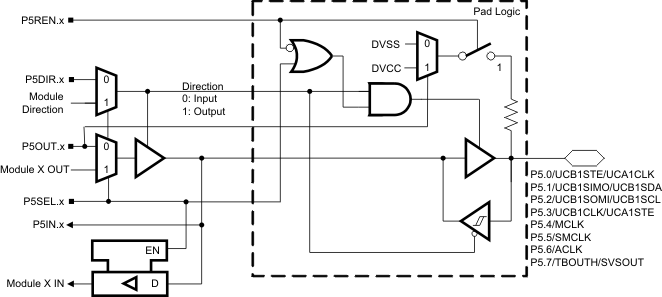 Figure 6-6 Port P5 (P5.0 to P5.7) Pin Schematics
Table 6-6 Port P5 (P5.0 to P5.7) Pin Functions
| PIN NAME (P5.X) | X | FUNCTION | CONTROL BITS/SIGNALS(1) | |
|---|---|---|---|---|
| P5DIR.x | P5SEL.x | |||
| P5.0/UCB1STE/UCA1CLK | 0 | P5.0 (I/O) | I: 0; O: 1 | 0 |
| UCB1STE/UCA1CLK(2)(3) | X | 1 | ||
| P5.1/UCB1SIMO/UCB1SDA | 1 | P5.1 (I/O) | I: 0; O: 1 | 0 |
| UCB1SIMO/UCB1SDA(2)(4) | X | 1 | ||
| P5.2/UCB1SOMI/UCB1SCL | 2 | P5.2 (I/O) | I: 0; O: 1 | 0 |
| UCB1SOMI/UCB1SCL(2)(4) | X | 1 | ||
| P5.3/UCB1CLK/UCA1STE | 3 | P5.3 (I/O) | I: 0; O: 1 | 0 |
| UCB1CLK/UCA1STE(2) | X | 1 | ||
| P5.4/MCLK | 4 | P5.0 (I/O) | I: 0; O: 1 | 0 |
| MCLK | 1 | 1 | ||
| P5.5/SMCLK | 5 | P5.1 (I/O) | I: 0; O: 1 | 0 |
| SMCLK | 1 | 1 | ||
| P5.6/ACLK | 6 | P5.2 (I/O) | I: 0; O: 1 | 0 |
| ACLK | 1 | 1 | ||
| P5.7/TBOUTH/SVSOUT | 7 | P5.7 (I/O) | I: 0; O: 1 | 0 |
| TBOUTH | 0 | 1 | ||
| SVSOUT | 1 | 1 | ||
6.7 Port P6 Pin Schematic: P6.0 to P6.4, Input/Output With Schmitt Trigger
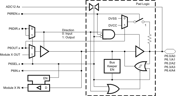 Figure 6-7 Port P6 (P6.0 to P6.4) Pin Schematic
Table 6-7 Port P6 (P6.0 to P6.4) Pin Functions
| PIN NAME (P6.X) | X | FUNCTION | CONTROL BITS/SIGNALS(1) | |
|---|---|---|---|---|
| P6DIR.x | P6SEL.x | |||
| P6.0/A0 | 0 | P6.0 (I/O) | I: 0; O: 1 | 0 |
| A0(2) | X | X | ||
| P6.1/A1 | 1 | P6.1 (I/O) | I: 0; O: 1 | 0 |
| A1(2) | X | X | ||
| P6.2/A2 | 2 | P6.2 (I/O) | I: 0; O: 1 | 0 |
| A2(2) | X | X | ||
| P6.3/A3 | 3 | P6.3(I/O) | I: 0; O: 1 | 0 |
| A3(2) | X | X | ||
| P6.4/A4 | 4 | P6.3 (I/O) | I: 0; O: 1 | 0 |
| A4(2) | X | X | ||
6.8 Port P6 Pin Schematic: P6.5 and P6.6, Input/Output With Schmitt Trigger
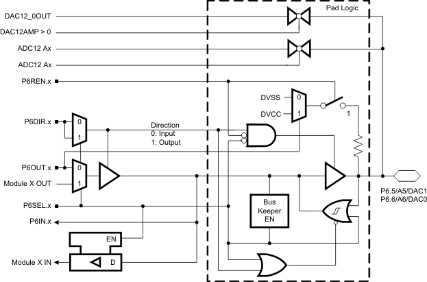 Figure 6-8 Port P6 (P6.5 to P6.6) Pin Schematic
Table 6-8 Port P6 (P6.5 to P6.6) Pin Functions
| PIN NAME (P6.X) | X | FUNCTION | CONTROL BITS/SIGNALS(1) | ||
|---|---|---|---|---|---|
| P6DIR.x | P6SEL.x | CAPD.x or DAC12AMP > 0 |
|||
| P6.5/A5/DAC1 | 5 | P6.5 (I/O) | I: 0; O: 1 | 0 | 0 |
| DVSS | 1 | 1 | 0 | ||
| A5(2) | X | X | 1 | ||
| DAC1 (DA12OPS = 1)(3) | X | X | 1 | ||
| P6.6/A6/DAC0 | 6 | P6.6 (I/O) | I: 0; O: 1 | 0 | 0 |
| DVSS | 1 | 1 | 0 | ||
| A6(2) | X | X | 1 | ||
| DAC1 (DA12OPS = 0)(3) | X | X | 1 | ||
6.9 Port P6 Pin Schematic: P6.7, Input/Output With Schmitt Trigger
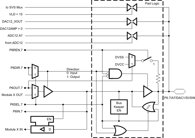 Figure 6-9 Port P6 (P6.7) Pin Schematic
Table 6-9 Port P6 (P6.7) Pin Functions
| PIN NAME (P6.X) | X | FUNCTION | CONTROL BITS/SIGNALS(1) | |
|---|---|---|---|---|
| P6DIR.x | P6SEL.x | |||
| P6.7/A7/DAC1/SVSIN | 7 | P6.7 (I/O) | I: 0; O: 1 | 0 |
| DVSS | 1 | 1 | ||
| A7(2) | X | X | ||
| DAC1 (DA12OPS = 0)(3) | X | X | ||
| SVSIN (VLD = 15) | X | X | ||
6.10 Port P7 Pin Schematic: P7.0 to P7.7, Input/Output With Schmitt Trigger
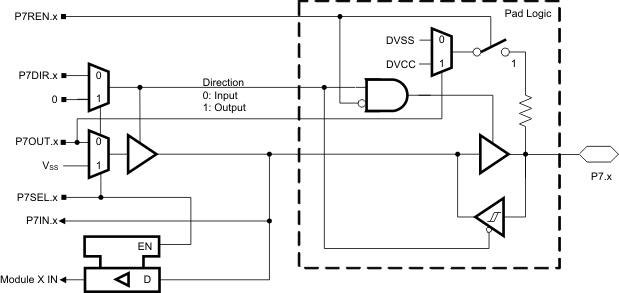 Figure 6-10 Port P7 (P7.0 to P7.7) Pin Schematic
Table 6-10 Port P7 (P7.0 to P7.7) Pin Functions(1)
| PIN NAME (P7.X) | X | FUNCTION | CONTROL BITS/SIGNALS | |
|---|---|---|---|---|
| P7DIR.x | P7SEL.x | |||
| P7.0 | 0 | P7.0 (I/O) | I: 0; O: 1 | 0 |
| Input | X | 1 | ||
| P7.1 | 1 | P7.1 (I/O) | I: 0; O: 1 | 0 |
| Input | X | 1 | ||
| P7.2 | 2 | P7.2 (I/O) | I: 0; O: 1 | 0 |
| Input | X | 1 | ||
| P7.3 | 3 | P7.3 (I/O) | I: 0; O: 1 | 0 |
| Input | X | 1 | ||
| P7.4 | 4 | P7.4 (I/O) | I: 0; O: 1 | 0 |
| Input | X | 1 | ||
| P7.5 | 5 | P7.5 (I/O) | I: 0; O: 1 | 0 |
| Input | X | 1 | ||
| P7.6 | 6 | P7.6 (I/O) | I: 0; O: 1 | 0 |
| Input | X | 1 | ||
| P7.7 | 7 | P7.7 (I/O) | I: 0; O: 1 | 0 |
| Input | X | 1 | ||
6.11 Port P8 Pin Schematic: P8.0 to P8.5, Input/Output With Schmitt Trigger
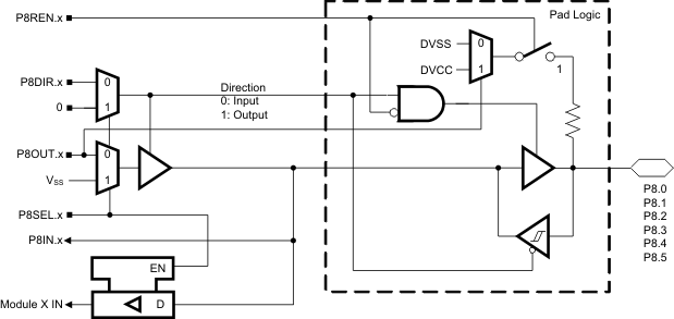 Figure 6-11 Port P8 (P8.0 to P8.5) Pin Schematic
Table 6-11 Port P8 (P8.0 to P8.5) Pin Functions(1)
| PIN NAME (P8.X) | X | FUNCTION | CONTROL BITS/SIGNALS | |
|---|---|---|---|---|
| P8DIR.x | P8SEL.x | |||
| P8.0 | 0 | P8.0 (I/O) | I: 0; O: 1 | 0 |
| Input | X | 1 | ||
| P8.1 | 1 | P8.1 (I/O) | I: 0; O: 1 | 0 |
| Input | X | 1 | ||
| P8.2 | 2 | P8.2 (I/O) | I: 0; O: 1 | 0 |
| Input | X | 1 | ||
| P8.3 | 3 | P8.3 (I/O) | I: 0; O: 1 | 0 |
| Input | X | 1 | ||
| P8.4 | 4 | P8.4 (I/O) | I: 0; O: 1 | 0 |
| Input | X | 1 | ||
| P8.5 | 5 | P8.5 (I/O) | I: 0; O: 1 | 0 |
| Input | X | 1 | ||
6.12 Port P8 Pin Schematic: P8.6, Input/Output With Schmitt Trigger
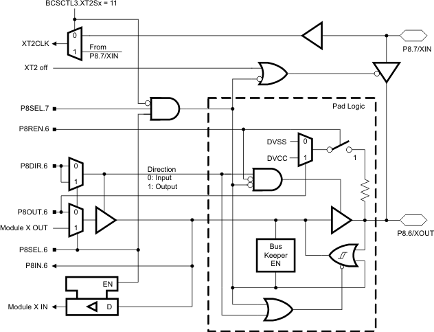 Figure 6-12 Port P8 (P8.6) Pin Schematic
Table 6-12 Port P8 (P8.6) Pin Functions(1)
| PIN NAME (P8.X) | X | FUNCTION | CONTROL BITS/SIGNALS | |
|---|---|---|---|---|
| P8DIR.x | P8SEL.x | |||
| P8.6/XOUT | 6 | P8.6 (I/O) | I: 0; O: 1 | 0 |
| XOUT (default) | 0 | 1 | ||
| DVSS | 1 | 1 | ||
6.13 Port P8 Pin Schematic: P8.7, Input/Output With Schmitt Trigger
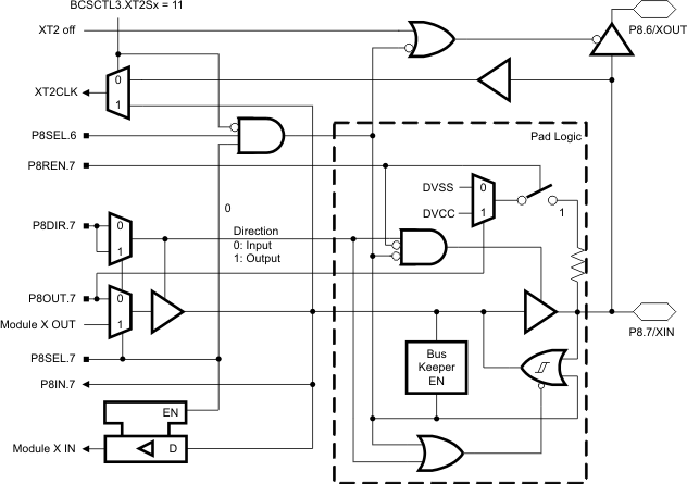 Figure 6-13 Port P8 (P8.7) Pin Schematic
Table 6-13 Port P8 (P8.7) Pin Functions(1)
| PIN NAME (P8.X) | X | FUNCTION | CONTROL BITS/SIGNALS | |
|---|---|---|---|---|
| P8DIR.x | P8SEL.x | |||
| P8.7/XIN | 6 | P8.7 (I/O) | I: 0; O: 1 | 0 |
| XIN (default) | 0 | 1 | ||
| VSS | 1 | 1 | ||
6.14 JTAG Pins: TMS, TCK, TDI/TCLK, TDO/TDI, Input/Output With Schmitt Trigger
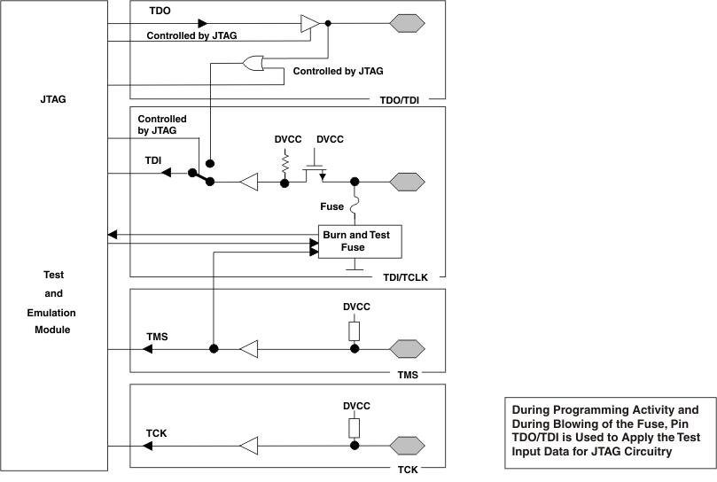 Figure 6-14 JTAG Module
6.15 JTAG Fuse Check Mode
MSP430 devices that have the fuse on the TEST terminal have a fuse check mode that tests the continuity of the fuse the first time the JTAG port is accessed after a power-on reset (POR). When activated, a fuse check current, ITF , of 1 mA at 3 V, 2.5 mA at 5 V can flow from the TEST pin to ground if the fuse is not burned. Care must be taken to avoid accidentally activating the fuse check mode and increasing overall system power consumption.
When the TEST pin is again taken low after a test or programming session, the fuse check mode and sense currents are terminated.
Activation of the fuse check mode occurs with the first negative edge on the TMS pin after power up or if TMS is being held low during power up. The second positive edge on the TMS pin deactivates the fuse check mode. After deactivation, the fuse check mode remains inactive until another POR occurs. After each POR the fuse check mode has the potential to be activated.
The fuse check current flows only when the fuse check mode is active and the TMS pin is in a low state (see Figure 6-15). Therefore, the additional current flow can be prevented by holding the TMS pin high (default condition).
 Figure 6-15 Fuse Check Mode Current