SLASE32C August 2014 – August 2018 MSP430FR5887 , MSP430FR5888 , MSP430FR5889 , MSP430FR58891 , MSP430FR6887 , MSP430FR6888 , MSP430FR6889 , MSP430FR68891
PRODUCTION DATA.
- 1Device Overview
- 2Revision History
- 3Device Comparison
- 4Terminal Configuration and Functions
-
5Specifications
- 5.1 Absolute Maximum Ratings
- 5.2 ESD Ratings
- 5.3 Recommended Operating Conditions
- 5.4 Active Mode Supply Current Into VCC Excluding External Current
- 5.5 Typical Characteristics, Active Mode Supply Currents
- 5.6 Low-Power Mode (LPM0, LPM1) Supply Currents Into VCC Excluding External Current
- 5.7 Low-Power Mode (LPM2, LPM3, LPM4) Supply Currents (Into VCC) Excluding External Current
- 5.8 Low-Power Mode With LCD Supply Currents (Into VCC) Excluding External Current
- 5.9 Low-Power Mode LPMx.5 Supply Currents (Into VCC) Excluding External Current
- 5.10 Typical Characteristics, Low-Power Mode Supply Currents
- 5.11 Typical Characteristics, Current Consumption per Module
- 5.12 Thermal Resistance Characteristics
- 5.13
Timing and Switching Characteristics
- 5.13.1 Power Supply Sequencing
- 5.13.2 Reset Timing
- 5.13.3 Clock Specifications
- 5.13.4 Wake-up Characteristics
- 5.13.5
Peripherals
- 5.13.5.1 Digital I/Os
- 5.13.5.2 Timer_A and Timer_B
- 5.13.5.3 eUSCI
- 5.13.5.4 LCD Controller
- 5.13.5.5
ADC
- Table 5-24 12-Bit ADC, Power Supply and Input Range Conditions
- Table 5-25 12-Bit ADC, Timing Parameters
- Table 5-26 12-Bit ADC, Linearity Parameters With External Reference
- Table 5-27 12-Bit ADC, Dynamic Performance for Differential Inputs With External Reference
- Table 5-28 12-Bit ADC, Dynamic Performance for Differential Inputs With Internal Reference
- Table 5-29 12-Bit ADC, Dynamic Performance for Single-Ended Inputs With External Reference
- Table 5-30 12-Bit ADC, Dynamic Performance for Single-Ended Inputs With Internal Reference
- Table 5-31 12-Bit ADC, Dynamic Performance With 32.768-kHz Clock
- Table 5-32 12-Bit ADC, Temperature Sensor and Built-In V1/2
- Table 5-33 12-Bit ADC, External Reference
- 5.13.5.6 Reference
- 5.13.5.7 Comparator
- 5.13.5.8
Scan Interface
- Table 5-36 Extended Scan Interface, Port Drive, Port Timing
- Table 5-37 Extended Scan Interface, Sample Capacitor/Ri Timing
- Table 5-38 Extended Scan Interface, VCC/2 Generator
- Table 5-39 Extended Scan Interface, 12-Bit DAC
- Table 5-40 Extended Scan Interface, Comparator
- Table 5-41 Extended Scan Interface, ESICLK Oscillator and TSM Clock Signals
- 5.13.5.9 FRAM Controller
- 5.13.6 Emulation and Debug
-
6Detailed Description
- 6.1 Overview
- 6.2 CPU
- 6.3 Operating Modes
- 6.4 Interrupt Vector Table and Signatures
- 6.5 Bootloader (BSL)
- 6.6 JTAG Operation
- 6.7 FRAM
- 6.8 RAM
- 6.9 Tiny RAM
- 6.10 Memory Protection Unit Including IP Encapsulation
- 6.11
Peripherals
- 6.11.1 Digital I/O
- 6.11.2 Oscillator and Clock System (CS)
- 6.11.3 Power-Management Module (PMM)
- 6.11.4 Hardware Multiplier (MPY)
- 6.11.5 Real-Time Clock (RTC_C)
- 6.11.6 Watchdog Timer (WDT_A)
- 6.11.7 System Module (SYS)
- 6.11.8 DMA Controller
- 6.11.9 Enhanced Universal Serial Communication Interface (eUSCI)
- 6.11.10 Extended Scan Interface (ESI)
- 6.11.11 Timer_A TA0, Timer_A TA1
- 6.11.12 Timer_A TA2
- 6.11.13 Timer_A TA3
- 6.11.14 Timer_B TB0
- 6.11.15 ADC12_B
- 6.11.16 Comparator_E
- 6.11.17 CRC16
- 6.11.18 CRC32
- 6.11.19 True Random Seed
- 6.11.20 Shared Reference (REF_A)
- 6.11.21 LCD_C
- 6.11.22 Embedded Emulation
- 6.11.23
Input/Output Diagrams
- 6.11.23.1 Digital I/O Functionality – Ports P1 to P10
- 6.11.23.2 Capacitive Touch Functionality Ports P1 to P10 and PJ
- 6.11.23.3 Port P1 (P1.0 to P1.3) Input/Output With Schmitt Trigger
- 6.11.23.4 Port P1 (P1.4 to P1.7) Input/Output With Schmitt Trigger
- 6.11.23.5 Port P2 (P2.0 to P2.3) Input/Output With Schmitt Trigger
- 6.11.23.6 Port P2 (P2.4 to P2.7) Input/Output With Schmitt Trigger
- 6.11.23.7 Port P3 (P3.0 to P3.7) Input/Output With Schmitt Trigger
- 6.11.23.8 Port P4 (P4.0 to P4.7) Input/Output With Schmitt Trigger
- 6.11.23.9 Port P5 (P5.0 to P5.7) Input/Output With Schmitt Trigger
- 6.11.23.10 Port P6 (P6.0 to P6.6) Input/Output With Schmitt Trigger
- 6.11.23.11 Port P6 (P6.7) Input/Output With Schmitt Trigger
- 6.11.23.12 Port P7 (P7.0 to P7.7) Input/Output With Schmitt Trigger
- 6.11.23.13 Port P8 (P8.0 to P8.3) Input/Output With Schmitt Trigger
- 6.11.23.14 Port P8 (P8.4 to P8.7) Input/Output With Schmitt Trigger
- 6.11.23.15 Port P9 (P9.0 to P9.3) Input/Output With Schmitt Trigger
- 6.11.23.16 Port P9 (P9.4 to P9.7) Input/Output With Schmitt Trigger
- 6.11.23.17 Port P10 (P10.0 to P10.2) Input/Output With Schmitt Trigger
- 6.11.23.18 Port PJ (PJ.4 and PJ.5) Input/Output With Schmitt Trigger
- 6.11.23.19 Port PJ (PJ.6 and PJ.7) Input/Output With Schmitt Trigger
- 6.11.23.20 Port PJ (PJ.0 to PJ.3) JTAG Pins TDO, TMS, TCK, TDI/TCLK, Input/Output With Schmitt Trigger
- 6.12 Device Descriptors (TLV)
- 6.13 Memory
- 6.14 Identification
- 7Applications, Implementation, and Layout
- 8Device and Documentation Support
- 9Mechanical, Packaging, and Orderable Information
Package Options
Mechanical Data (Package|Pins)
Thermal pad, mechanical data (Package|Pins)
- PZ|100
Orderable Information
1.4 Functional Block Diagram
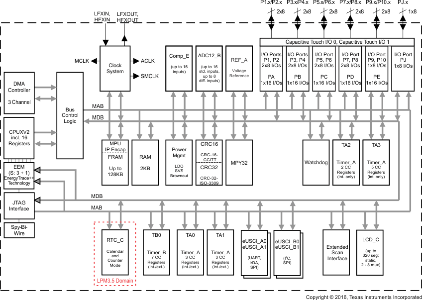
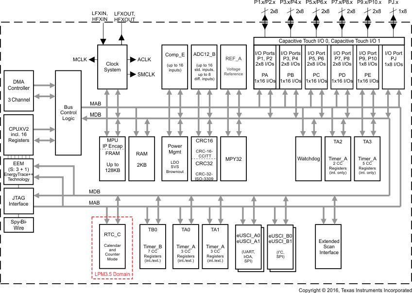
Figure 1-1 and Figure 1-2 show the functional block diagrams.
 Figure 1-1 Functional Block Diagram – MSP430FR688x, MSP430FR688x1
  Figure 1-2 Functional Block Diagram – MSP430FR588x, MSP430FR588x1