SLLSEK1B July 2014 – March 2018 ONET2804T
PRODUCTION DATA.
- 1 Features
- 2 Applications
- 3 Description
- 4 Revision History
- 5 Pin Configuration and Functions
- 6 Specifications
-
7 Detailed Description
- 7.1 Overview
- 7.2 Functional Block Diagram
- 7.3 Feature Description
- 7.4 Device Functional Modes
- 7.5
Register Maps
- 7.5.1 Register 0 (0x00) – Control Settings (offset = 0h) [reset = 0h]
- 7.5.2 Register 1 (0x01) – Amplitude and Rate for Channel 1 (offset = 1h) [reset = 0h]
- 7.5.3 Register 2 (0x02) Mapping – Threshold and Gain for Channel 1 (offset = 2h) [reset = 0h]
- 7.5.4 Register 3 (0x03) – Reserved
- 7.5.5 Register 4 (0x04) – Reserved
- 7.5.6 Register 5 (0x05) – Reserved
- 7.5.7 Register 6 (0x06) – Reserved
- 7.5.8 Register 7 (0x07) – Amplitude and Rate for Channel 2 (offset = 7h) [reset = 0h]
- 7.5.9 Register 8 (0x08) Mapping – Threshold and Gain for Channel 1 (offset = 8h) [reset = 0h]
- 7.5.10 Register 9 (0x09) – Reserved
- 7.5.11 Register 10 (0x0A) – Reserved
- 7.5.12 Register 11 (0x0B) – Reserved
- 7.5.13 Register 12 (0x0C) – Reserved
- 7.5.14 Register 13 (0x0D) – Amplitude and Rate for Channel 3 (offset = Dh) [reset = 0h]
- 7.5.15 Register 14 (0x0E) Mapping – Threshold and Gain for Channel 3 (offset = Eh) [reset = 0h]
- 7.5.16 Register 15 (0x0F) – Reserved
- 7.5.17 Register 16 (0x10) – Reserved
- 7.5.18 Register 17 (0x11) – Reserved
- 7.5.19 Register 18 (0x12) – Reserved
- 7.5.20 Register 19 (0x13) – Amplitude and Rate for Channel 4 (offset = 13h ) [reset = 0h]
- 7.5.21 Register 20 (0x14) Mapping – Threshold and Gain for Channel 4 (offset =14h) [reset = 0h]
- 7.5.22 Register 21 (0x15) – Reserved
- 7.5.23 Register 22 (0x10) – Reserved
- 7.5.24 Register 23 (0x17) – Reserved
- 7.5.25 Register 24 (0x18) – Reserved
- 7.5.26 Register 25 (0x19) – Reserved
- 8 Application and Implementation
- 9 Power Supply Recommendations
- 10Layout
- 11Device and Documentation Support
- 12Mechanical, Packaging, and Orderable Information
Package Options
Mechanical Data (Package|Pins)
- Y|0
Thermal pad, mechanical data (Package|Pins)
Orderable Information
7.4.8 Acknowledge
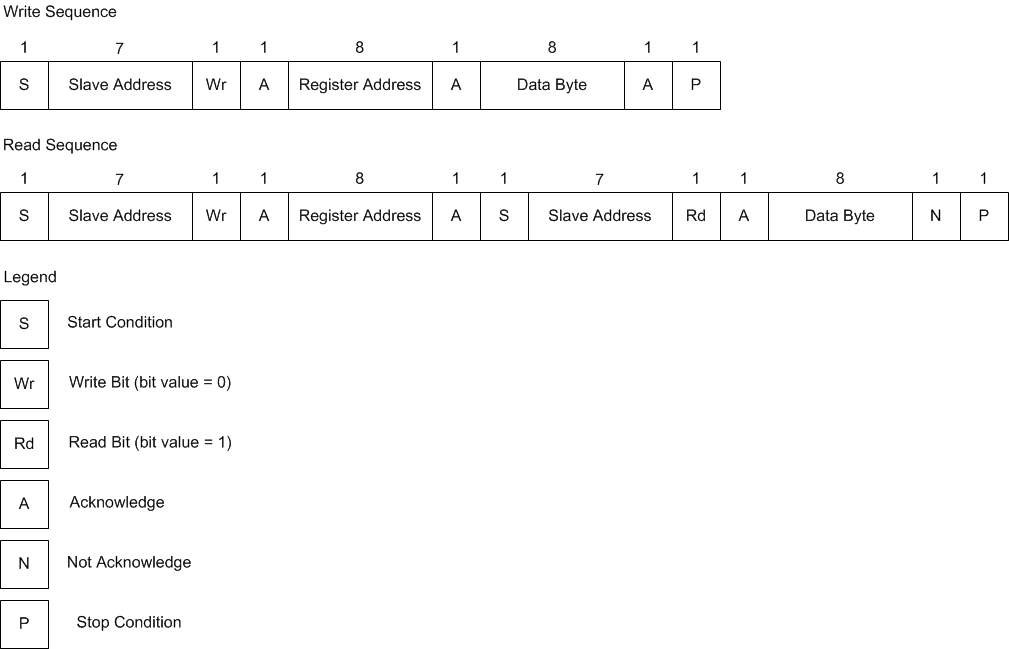
Each receiving device, when addressed, is obliged to generate an acknowledge bit. The transmitter releases the SDA line and a device that acknowledges must pull down the SDA line during the acknowledge clock pulse in such a way that the SDA line is stable LOW during the HIGH period of the acknowledge clock pulse. Setup and hold times must be taken into account. When a slave-receiver does not acknowledge the slave address, the data line must be left HIGH by the slave. The master can then generate a STOP condition to abort the transfer. If the slave-receiver does acknowledge the slave address but some time later in the transfer cannot receive any more data bytes, the master must abort the transfer. This is indicated by the slave generating the not acknowledge on the first byte to follow. The slave leaves the data line HIGH and the master generates the STOP condition.
 Figure 14. I2C Timing Diagram
Table 1. Timing Diagram Definitions
| MIN | MAX | UNIT | ||
|---|---|---|---|---|
| fSCK | SCK clock frequency | 400 | kHz | |
| tBUF | Bus free time between START and STOP conditions | 1.3 | µs | |
| tHDSTA | Hold time after repeated START condition. After this period, the first clock pulse is generated | 0.6 | µs | |
| tLOW | Low period of the SCK clock | 1.3 | µs | |
| tHIGH | High period of the SCK clock | 0.6 | µs | |
| tSUSTA | Setup time for a repeated START condition | 0.6 | µs | |
| tHDDAT | Data HOLD time | 0 | µs | |
| tSUDAT | Data setup time | 100 | ns | |
| tR | Rise time of both SDA and SCK signals | 300 | ns | |
| tF | Fall time of both SDA and SCK signals | 300 | ns | |
| tSUSTO | Setup time for STOP condition | 0.6 | µs | |
 Figure 15. Data Transfer