SBOS618I December   2013  – May 2018 OPA172 , OPA2172 , OPA4172

PRODUCTION DATA.  

  1. Features
  2. Applications
  3. Description
    1.     Device Images
      1.      JFET-Input Low-Noise Amplifier
      2.      Superior THD Performance
  4. Revision History
  5. Device Comparison
    1. 5.1 Device Comparison
    2. 5.2 Device Family Comparison
  6. Pin Configuration and Functions
    1.     Pin Functions: OPA172
    2.     Pin Functions: OPA2172 and OPA4172
  7. Specifications
    1. 7.1 Absolute Maximum Ratings
    2. 7.2 ESD Ratings
    3. 7.3 Recommended Operating Conditions
    4. 7.4 Thermal Information: OPA172
    5. 7.5 Thermal Information: OPA2172
    6. 7.6 Thermal Information: OPA4172
    7. 7.7 Electrical Characteristics
    8. 7.8 Typical Characteristics: Table of Graphs
    9. 7.9 Typical Characteristics
  8. Detailed Description
    1. 8.1 Overview
    2. 8.2 Functional Block Diagram
    3. 8.3 Feature Description
      1. 8.3.1 EMI Rejection
      2. 8.3.2 Phase-Reversal Protection
      3. 8.3.3 Capacitive Load and Stability
    4. 8.4 Device Functional Modes
      1. 8.4.1 Common-Mode Voltage Range
      2. 8.4.2 Electrical Overstress
      3. 8.4.3 Overload Recovery
  9. Applications and Implementation
    1. 9.1 Application Information
    2. 9.2 Typical Applications
      1. 9.2.1 Capacitive Load Drive Solution Using an Isolation Resistor
        1. 9.2.1.1 Design Requirements
        2. 9.2.1.2 Detailed Design Procedure
        3. 9.2.1.3 Application Curve
      2. 9.2.2 Bidirectional Current Source
      3. 9.2.3 JFET-Input Low-Noise Amplifier
  10. 10Power-Supply Recommendations
  11. 11Layout
    1. 11.1 Layout Guidelines
    2. 11.2 Layout Example
  12. 12Device and Documentation Support
    1. 12.1 Device Support
      1. 12.1.1 Development Support
        1. 12.1.1.1 TINA-TI (Free Software Download)
    2. 12.2 Documentation Support
      1. 12.2.1 Related Documentation
    3. 12.3 Related Links
    4. 12.4 Community Resources
    5. 12.5 Trademarks
    6. 12.6 Electrostatic Discharge Caution
    7. 12.7 Glossary
  13. 13Mechanical, Packaging, and Orderable Information

Package Options

Mechanical Data (Package|Pins)
Thermal pad, mechanical data (Package|Pins)
Orderable Information

Capacitive Load and Stability

The dynamic characteristics of the OPAx172 are optimized for commonly-used operating conditions. The combination of low closed-loop gain and high capacitive loads decreases the phase margin of the amplifier and may lead to gain peaking or oscillations. As a result, heavier capacitive loads must be isolated from the output. The simplest way to achieve this isolation is to add a small resistor (for example, ROUT = 50 Ω) in series with the output. Figure 44 and Figure 45 show graphs of small-signal overshoot versus capacitive load for several values of ROUT. Refer to Application Bulletin SBOA015 (AB-028), Feedback Plots Define Op Amp AC Performance, available for download from www.ti.com, for details of analysis techniques and application circuits.
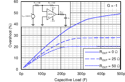
OPA172 OPA2172 OPA4172 C022_SBOS618.pngFigure 44. Small-Signal Overshoot vs Capacitive Load (100-mV Output Step)
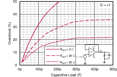
OPA172 OPA2172 OPA4172 C021_SBOS618.pngFigure 45. Small-Signal Overshoot vs Capacitive Load (100-mV Output Step)