SBOS618I December   2013  – May 2018 OPA172 , OPA2172 , OPA4172

PRODUCTION DATA.  

  1. Features
  2. Applications
  3. Description
    1.     Device Images
      1.      JFET-Input Low-Noise Amplifier
      2.      Superior THD Performance
  4. Revision History
  5. Device Comparison
    1. 5.1 Device Comparison
    2. 5.2 Device Family Comparison
  6. Pin Configuration and Functions
    1.     Pin Functions: OPA172
    2.     Pin Functions: OPA2172 and OPA4172
  7. Specifications
    1. 7.1 Absolute Maximum Ratings
    2. 7.2 ESD Ratings
    3. 7.3 Recommended Operating Conditions
    4. 7.4 Thermal Information: OPA172
    5. 7.5 Thermal Information: OPA2172
    6. 7.6 Thermal Information: OPA4172
    7. 7.7 Electrical Characteristics
    8. 7.8 Typical Characteristics: Table of Graphs
    9. 7.9 Typical Characteristics
  8. Detailed Description
    1. 8.1 Overview
    2. 8.2 Functional Block Diagram
    3. 8.3 Feature Description
      1. 8.3.1 EMI Rejection
      2. 8.3.2 Phase-Reversal Protection
      3. 8.3.3 Capacitive Load and Stability
    4. 8.4 Device Functional Modes
      1. 8.4.1 Common-Mode Voltage Range
      2. 8.4.2 Electrical Overstress
      3. 8.4.3 Overload Recovery
  9. Applications and Implementation
    1. 9.1 Application Information
    2. 9.2 Typical Applications
      1. 9.2.1 Capacitive Load Drive Solution Using an Isolation Resistor
        1. 9.2.1.1 Design Requirements
        2. 9.2.1.2 Detailed Design Procedure
        3. 9.2.1.3 Application Curve
      2. 9.2.2 Bidirectional Current Source
      3. 9.2.3 JFET-Input Low-Noise Amplifier
  10. 10Power-Supply Recommendations
  11. 11Layout
    1. 11.1 Layout Guidelines
    2. 11.2 Layout Example
  12. 12Device and Documentation Support
    1. 12.1 Device Support
      1. 12.1.1 Development Support
        1. 12.1.1.1 TINA-TI (Free Software Download)
    2. 12.2 Documentation Support
      1. 12.2.1 Related Documentation
    3. 12.3 Related Links
    4. 12.4 Community Resources
    5. 12.5 Trademarks
    6. 12.6 Electrostatic Discharge Caution
    7. 12.7 Glossary
  13. 13Mechanical, Packaging, and Orderable Information

Package Options

Mechanical Data (Package|Pins)
Thermal pad, mechanical data (Package|Pins)
Orderable Information

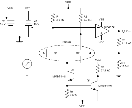
JFET-Input Low-Noise Amplifier

Figure 51 shows a low-noise composite amplifier built by adding a low noise JFET pair (Q1 and Q2) as an input preamplifier for the OPA172. Transistors Q3 and Q4 form a 2-mA current sink that biases each JFET with 1 mA of drain current. Using 3.9-kΩ drain resistors produces a gain of approximately 10 in the input amplifier, making the extremely-low, broadband-noise spectral density of the JFET pair, Q1 and Q2, the dominant noise source of the amplifier. The output impedance of the input differential amplifier is large enough that a FET-input amplifier such as the OPA172 provides superior noise performance over bipolar-input amplifiers.

The gain of the composite amplifier is given by Equation 3:

Equation 3. AV = (1 + R3 / R4)

The resistances shown are standard 1% resistor values that produce a gain of approximately 100 (99.26) with 68° of phase margin. Gains less than 10 may require additional compensation methods to provide stability. Select low resistor values to minimize the resistor thermal noise contribution to the total output noise.
OPA172 OPA2172 OPA4172 ai_lownoiseamp_bos618.gifFigure 51. JFET-Input Low-Noise Amplifier