SBOS642C March   2013  – January 2020 OPA188

PRODUCTION DATA.  

  1. Features
  2. Applications
  3. Description
    1.     Device Images
      1.      Auto-Zero Technology Provides Ultra-Low Temperature Drift
  4. Revision History
  5. Device Comparison Table
    1. 5.1 Portfolio Comparison
  6. Pin Configuration and Functions
    1.     Pin Functions
  7. Specifications
    1. 7.1 Absolute Maximum Ratings
    2. 7.2 ESD Ratings
    3. 7.3 Recommended Operating Conditions
    4. 7.4 Thermal Information
    5. 7.5 Electrical Characteristics: High-Voltage Operation
    6. 7.6 Electrical Characteristics: Low-Voltage Operation
    7. 7.7 Typical Characteristics: Table of Graphs
      1. 7.7.1 Table of Graphs
    8. 7.8 Typical Characteristics
  8. Detailed Description
    1. 8.1 Overview
    2. 8.2 Functional Block Diagram
    3. 8.3 Feature Description
      1. 8.3.1 Operating Characteristics
      2. 8.3.2 Phase-Reversal Protection
      3. 8.3.3 Input Bias Current Clock Feedthrough
      4. 8.3.4 Internal Offset Correction
      5. 8.3.5 EMI Rejection
      6. 8.3.6 Capacitive Load and Stability
      7. 8.3.7 Electrical Overstress
    4. 8.4 Device Functional Modes
  9. Application and Implementation
    1. 9.1 Application Information
    2. 9.2 Typical Applications
      1. 9.2.1 High-Side Voltage-to-Current (V-I) Converter
        1. 9.2.1.1 Design Requirements
        2. 9.2.1.2 Detailed Design Procedure
        3. 9.2.1.3 Application Curves
      2. 9.2.2 Discrete INA + Attenuation for ADC With 3.3-V Supply
      3. 9.2.3 Bridge Amplifier
      4. 9.2.4 Low-Side Current Monitor
      5. 9.2.5 Programmable Power Supply
      6. 9.2.6 RTD Amplifier With Linearization
  10. 10Power Supply Recommendations
  11. 11Layout
    1. 11.1 Layout Guidelines
    2. 11.2 Layout Example
  12. 12Device and Documentation Support
    1. 12.1 Device Support
      1. 12.1.1 Development Support
        1. 12.1.1.1 TINA-TI (Free Download Software)
    2. 12.2 Documentation Support
      1. 12.2.1 Related Documentation
    3. 12.3 Receiving Notification of Documentation Updates
    4. 12.4 Support Resources
    5. 12.5 Trademarks
    6. 12.6 Electrostatic Discharge Caution
    7. 12.7 Glossary
  13. 13Mechanical, Packaging, and Orderable Information

Package Options

Mechanical Data (Package|Pins)
Thermal pad, mechanical data (Package|Pins)
Orderable Information

Programmable Power Supply

Figure 49 shows the OPA188 configured as a precision programmable power supply using the 16-bit, voltage output DAC8581 and the OPA548 high-current amplifier. This application amplifies the digital-to-analog converter (DAC) voltage by a value of five, and handles a large variety of capacitive and current loads. The OPA188 in the front-end provides precision and low drift across a wide range of inputs and conditions. Click the following link to download the TINA-TI file: Programmable Power-Supply Circuit.
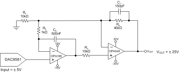
OPA188 SBOS642Fig46.gifFigure 49. Programmable Power Supply