SBOS812H October   2017  – May 2020 OPA202 , OPA2202 , OPA4202

PRODUCTION DATA.  

  1. Features
  2. Applications
  3. Description
    1.     Device Images
      1.      OPAx202 Excel Even When Directly Driving Heavy Capacitive Loads
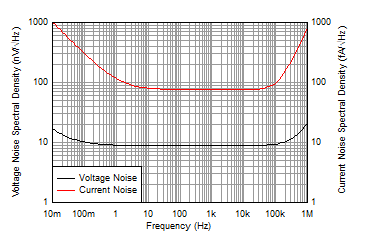
      2.      Input Voltage Noise and Current Noise Spectral Density vs Frequency
  4. Revision History
  5. Pin Configuration and Functions
    1.     Pin Functions: OPA202
    2.     Pin Functions: OPA2202
    3.     Pin Functions: OPA4202
  6. Specifications
    1. 6.1 Absolute Maximum Ratings
    2. 6.2 ESD Ratings
    3. 6.3 Recommended Operating Conditions
    4. 6.4 Thermal Information: OPA202
    5. 6.5 Thermal Information: OPA2202
    6. 6.6 Thermal Information: OPA4202
    7. 6.7 Electrical Characteristics
    8. 6.8 Typical Characteristics
    9. 6.9 Typical Characteristics
  7. Detailed Description
    1. 7.1 Overview
    2. 7.2 Functional Block Diagram
    3. 7.3 Feature Description
      1. 7.3.1 Capacitive Load and Stability
      2. 7.3.2 Output Current Limit
      3. 7.3.3 Noise Performance
      4. 7.3.4 Phase-Reversal Protection
      5. 7.3.5 Thermal Protection
      6. 7.3.6 Electrical Overstress
      7. 7.3.7 EMI Rejection
      8. 7.3.8 EMIRR +IN Test Configuration
    4. 7.4 Device Functional Modes
  8. Application and Implementation
    1. 8.1 Application Information
      1. 8.1.1 Basic Noise Calculations
    2. 8.2 Typical Application
      1. 8.2.1 Design Requirements
      2. 8.2.2 Detailed Design Procedure
      3. 8.2.3 Application Curve
  9. Power Supply Recommendations
  10. 10Layout
    1. 10.1 Layout Guidelines
    2. 10.2 Layout Example
  11. 11Device and Documentation Support
    1. 11.1 Device Support
      1. 11.1.1 Development Support
        1. 11.1.1.1 TINA-TI (Free Software Download)
        2. 11.1.1.2 WEBENCH Filter Designer Tool
        3. 11.1.1.3 TI Precision Designs
    2. 11.2 Documentation Support
      1. 11.2.1 Related Documentation
    3. 11.3 Related Links
    4. 11.4 Receiving Notification of Documentation Updates
    5. 11.5 Support Resources
    6. 11.6 Trademarks
    7. 11.7 Electrostatic Discharge Caution
    8. 11.8 Glossary
  12. 12Mechanical, Packaging, and Orderable Information

Package Options

Mechanical Data (Package|Pins)
Thermal pad, mechanical data (Package|Pins)
Orderable Information

Typical Characteristics

at TA = 25°C, VS = ±18 V, VCM = VS / 2, RLOAD = 10 kΩ connected to VS / 2, and CL = 100 pF (unless otherwise noted)
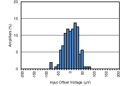
OPA202 OPA2202 OPA4202 C002_SBOS427.png
µ = –3.56 µV σ = 32.09 µV N = 252
Figure 1. Offset Voltage Production Distribution
OPA202 OPA2202 OPA4202 C015_SBOS427.png
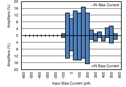
µ–IN = 112.335 pA σ–IN = 154.946 pA N = 90
µ+IN = 112.448 pA σ+IN = 152.739 pA
Figure 3. Input Bias Current Production Distribution
OPA202 OPA2202 OPA4202 C010_SBOS427.png
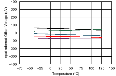
5 typical units
Figure 5. Offset Voltage vs Temperature
OPA202 OPA2202 OPA4202 C017_SBOS427.png
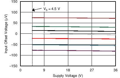
5 typical units
Figure 7. Offset Voltage vs Supply Voltage
OPA202 OPA2202 OPA4202 C202_SBOS427.png
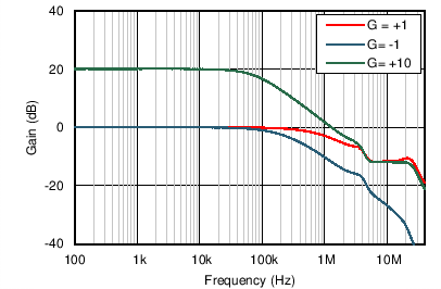
Figure 9. Closed-Loop Gain vs Frequency
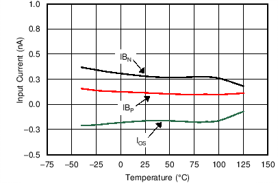
OPA202 OPA2202 OPA4202 C014_SBOS427.png
Figure 11. Input Bias Current and Offset vs Temperature
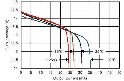
OPA202 OPA2202 OPA4202 C009A_SBOS427.png
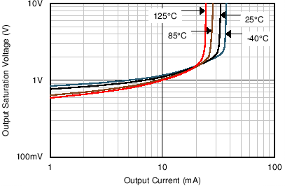
Figure 13. Output Voltage Swing vs Output Current (Sourcing)
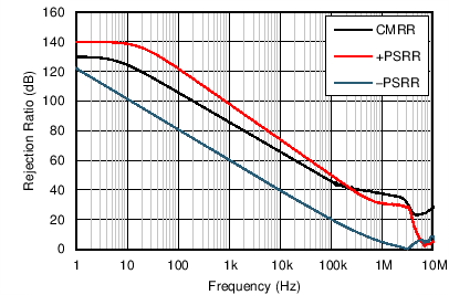
OPA202 OPA2202 OPA4202 C203_SBOS427.png
Figure 15. CMRR and PSRR vs Frequency
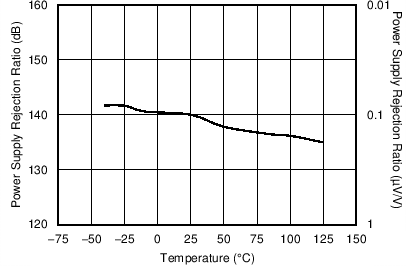
OPA202 OPA2202 OPA4202 C012_SBOS427.png
Figure 17. PSRR vs Temperature
OPA202 OPA2202 OPA4202 VoltageCurrentNoiseCurve.gif
Figure 19. Input Voltage Noise and Current Noise Spectral Density vs Frequency
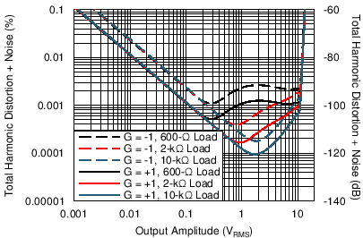
OPA202 OPA2202 OPA4202 C207_SBOS427.png
f = 1 kHz BW = 90 kHz
Figure 21. THD+N vs Output Amplitude
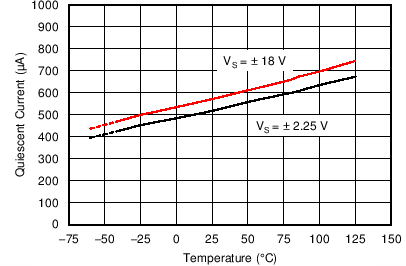
OPA202 OPA2202 OPA4202 C007_SBOS427.png
Figure 23. Quiescent Current vs Temperature
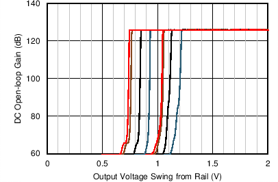
OPA202 OPA2202 OPA4202 C019_SBOS427.png
VS = ±18 V
Figure 25. Open-Loop Gain vs Output Voltage
Swing to Supply
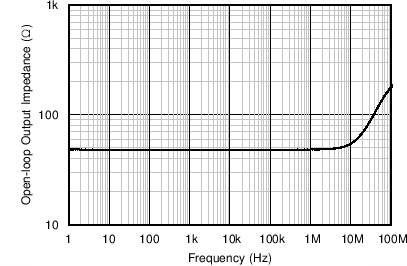
OPA202 OPA2202 OPA4202 C220_SBOS427.png
Unity-gain bandwidth = 1 MHz
Figure 27. Open-Loop Output Impedance vs Frequency
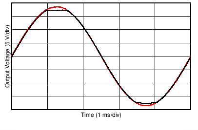
OPA202 OPA2202 OPA4202 C209_SBOS427.png
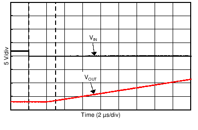
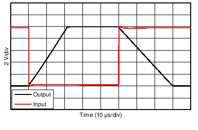
Figure 29. No Phase Reversal
OPA202 OPA2202 OPA4202 C210_SBOS727.png
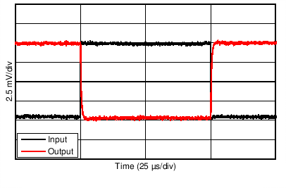
Figure 31. Negative Overload Recovery
OPA202 OPA2202 OPA4202 C215_SBOS427.png
G = –1
Figure 33. Small-Signal Step Response (10-mV Step)
OPA202 OPA2202 OPA4202 C212_SBOS427.png
G = +1 10-V step
Figure 35. Large-Signal Step Response
OPA202 OPA2202 OPA4202 C008_SBOS427.png
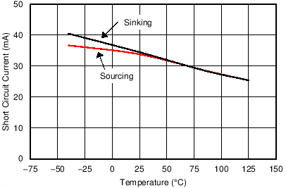
Figure 37. Short-Circuit Current vs Temperature
OPA202 OPA2202 OPA4202 C219_SBOS427.png
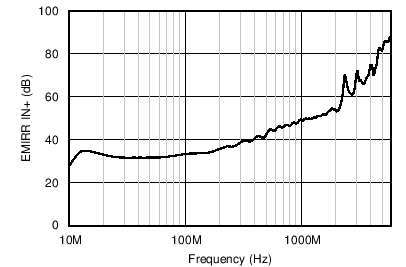
PRF = –10 dBm
Figure 39. EMIRR vs Frequency
OPA202 OPA2202 OPA4202 C001_SBOS427.png
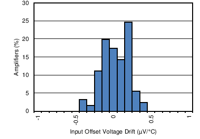
µ = –18.23 nV/°C σ = 177.41 nV/°C N = 252
TA = –40°C to +105°C
Figure 2. Offset Voltage Drift Distribution
OPA202 OPA2202 OPA4202 C016_SBOS427.png
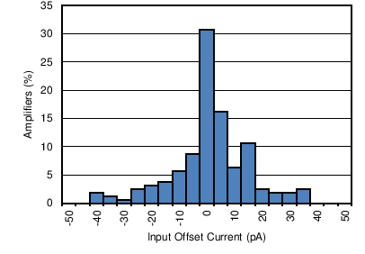
µ = 0.112 pA σ = 15.023 pA N = 90
Figure 4. Input Offset Current Production Distribution
OPA202 OPA2202 OPA4202 C003_SBOS427.png
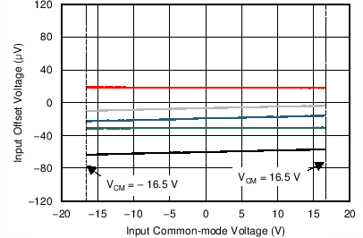
5 typical units
Figure 6. Offset Voltage vs Common-Mode Voltage
OPA202 OPA2202 OPA4202 C201_SBOS427.png
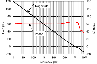
Figure 8. Open-Loop Gain and Phase vs Frequency
OPA202 OPA2202 OPA4202 C013_SBOS427.png
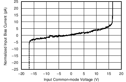
Figure 10. Input Bias Current vs Common-Mode Voltage
OPA202 OPA2202 OPA4202 C009C_SBOS427.png
Figure 12. Output Voltage Swing vs Output Current
OPA202 OPA2202 OPA4202 C009B_SBOS427.png
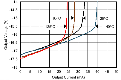
Figure 14. Output Voltage Swing vs Output Current (Sinking)
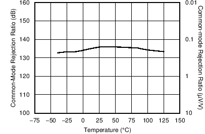
OPA202 OPA2202 OPA4202 C011_SBOS427.png
Figure 16. CMRR vs Temperature
OPA202 OPA2202 OPA4202 C204_SBOS427.png
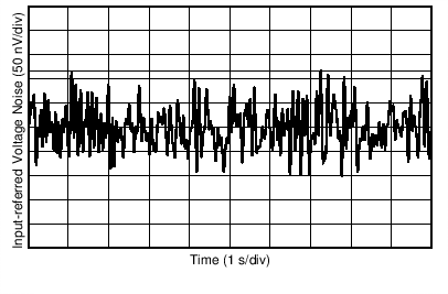
Figure 18. 0.1-Hz to 10-Hz Voltage Noise
OPA202 OPA2202 OPA4202 C206_SBOS427.png
VOUT = 3.5 VRMS BW = 90 kHz
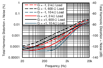
Figure 20. THD+N Ratio vs Frequency
OPA202 OPA2202 OPA4202 C004_SBOS427.png
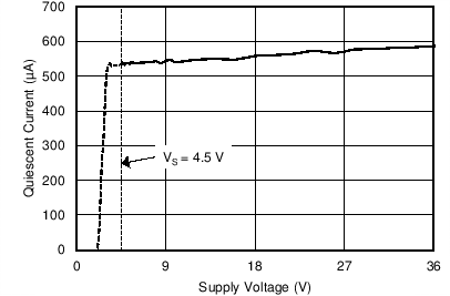
Figure 22. Quiescent Current vs Supply Voltage
OPA202 OPA2202 OPA4202 C005_SBOS427.png
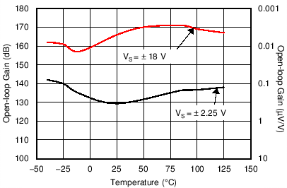
Figure 24. Open-Loop Gain vs Temperature
(With 10-kΩ Load)
OPA202 OPA2202 OPA4202 C018_SBOS427.png
VS = ±2.25 V
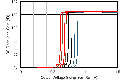
Figure 26. Open-Loop Gain vs Output Voltage Swing to Supply
OPA202 OPA2202 OPA4202 C208_SBOS427.png
10-mV step
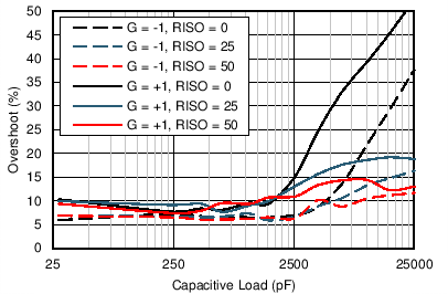
Figure 28. Small-Signal Overshoot vs Capacitive Load
OPA202 OPA2202 OPA4202 C211_SBOS727.png
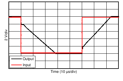
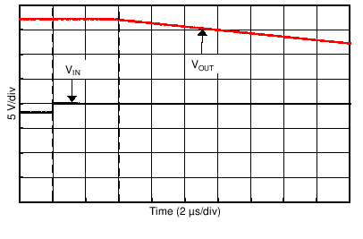
Figure 30. Positive Overload Recovery
OPA202 OPA2202 OPA4202 C214_SBOS427.png
G = +1
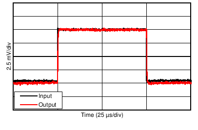
Figure 32. Small-Signal Step Response (10-mV Step)
OPA202 OPA2202 OPA4202 C213_SBOS427.png
G = –1 10-V step
Figure 34. Large-Signal Step Response
OPA202 OPA2202 OPA4202 C216_SBOS427.png
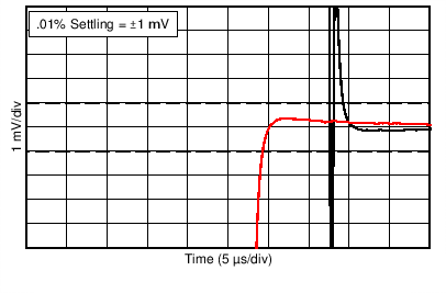
10-V step
Figure 36. Settling Time
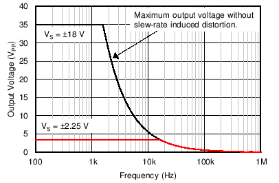
OPA202 OPA2202 OPA4202 C217_SBOS427.png
Figure 38. Maximum Output Voltage Amplitude vs Frequency