SBOS936E November 2019 – August 2022 OPA182 , OPA2182 , OPA4182
PRODMIX
- 1 Features
- 2 Applications
- 3 Description
- 4 Revision History
- 5 Device Comparison Table
- 6 Pin Configuration and Functions
- 7 Specifications
- 8 Detailed Description
- 9 Application and Implementation
- 10Device and Documentation Support
- 11Mechanical, Packaging, and Orderable Information
Package Options
Mechanical Data (Package|Pins)
Thermal pad, mechanical data (Package|Pins)
Orderable Information
7.8 Typical Characteristics
at TA = 25°C, VS = ±18 V, VCM = VS / 2, RLOAD = 10 kΩ connected to VS / 2, and CL = 100 pF (unless otherwise noted)
Table 7-1 Typical Characteristic Graphs
| DESCRIPTION | FIGURE |
|---|---|
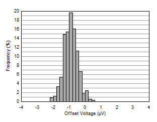
| Offset Voltage Production Distribution | Figure 7-1 |
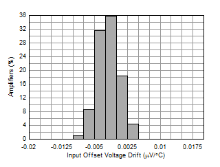
| Offset Voltage Drift Distribution From –40°C to 125°C | Figure 7-2 |
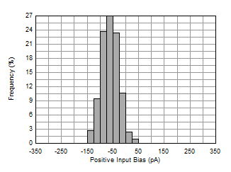
| Input Bias Current Production Distribution | Figure 7-3 |
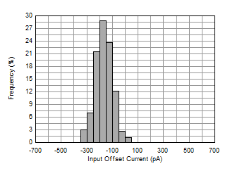
| Input Offset Current Production Distribution | Figure 7-4 |
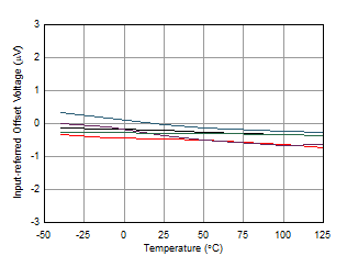
| Offset Voltage vs Temperature | Figure 7-5 |
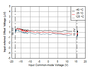
| Offset Voltage vs Common-Mode Voltage | Figure 7-6 |
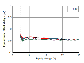
| Offset Voltage vs Supply Voltage | Figure 7-7 |
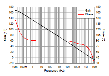
| Open-Loop Gain and Phase vs Frequency | Figure 7-8 |
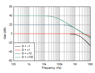
| Closed-Loop Gain vs Frequency | Figure 7-9 |
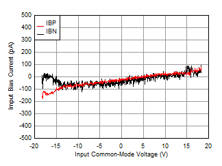
| Input Bias Current vs Common-Mode Voltage | Figure 7-10 |
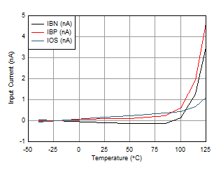
| Input Bias Current and Offset vs Temperature | Figure 7-11 |
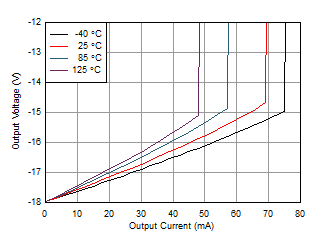
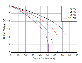
| Output Voltage Swing vs Output Current (Sourcing) | Figure 7-12 |
| Output Voltage Swing vs Output Current (Sinking) | Figure 7-13 |
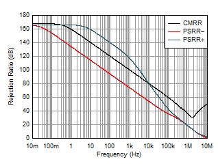
| CMRR and PSRR vs Frequency | Figure 7-14 |
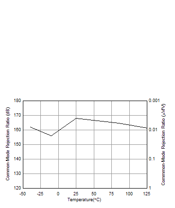
| CMRR vs Temperature | Figure 7-15 |
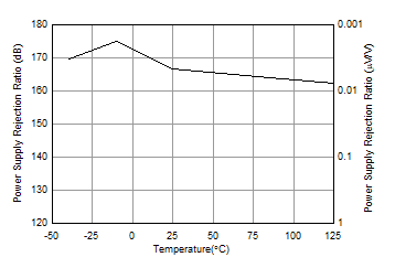
| PSRR vs Temperature | Figure 7-16 |
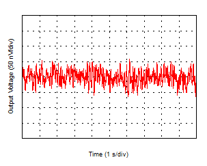
| 0.1-Hz to 10-Hz Voltage Noise | Figure 7-17 |
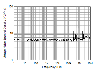
| Input Voltage Noise Spectral Density vs Frequency | Figure 7-18 |
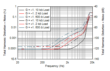
| THD+N Ratio vs Frequency | Figure 7-19 |
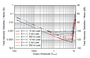
| THD+N vs Output Amplitude | Figure 7-20 |
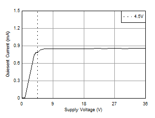
| Quiescent Current vs Supply Voltage | Figure 7-21 |
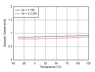
| Quiescent Current vs Temperature | Figure 7-22 |
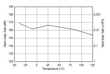
| Open-Loop Gain vs Temperature (10-kΩ) | Figure 7-23 |
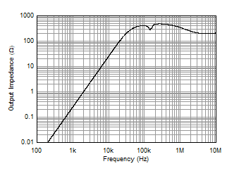
| Open-Loop Output Impedance vs Frequency | Figure 7-24 |
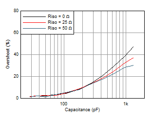
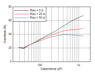
| Small-Signal Overshoot vs Capacitive Load (10-mV Step) | Figure 7-25, Figure 7-26 |
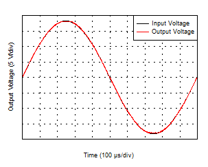
| No Phase Reversal | Figure 7-27 |
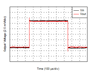
| Positive Overload Recovery | Figure 7-28 |
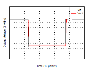
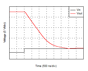
| Negative Overload Recovery | Figure 7-29 |
| Small-Signal Step Response (10-mV Step) | Figure 7-30, Figure 7-31 |
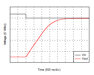
| Large-Signal Step Response (10-V Step) | Figure 7-32, Figure 7-33 |
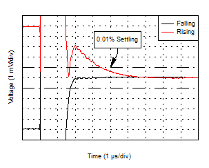
| Settling Time | Figure 7-34 |
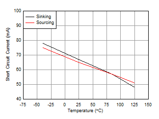
| Short Circuit Current vs Temperature | Figure 7-35 |
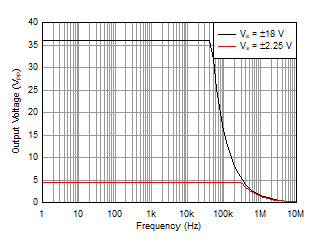
| Maximum Output Voltage vs Frequency | Figure 7-36 |
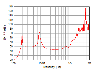
| EMIRR vs Frequency | Figure 7-37 |
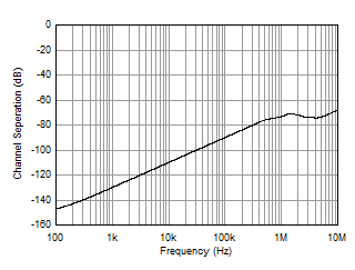
| Channel Separation | Figure 7-38 |
| Inverting Configuration |
| Noninverting Configuration |
| Noninverting Configuration |
| Noninverting Configuration |
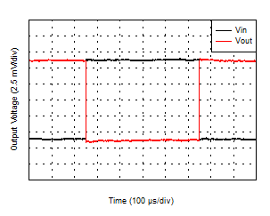
| Inverting Configuration |
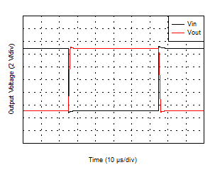
| Inverting Configuration |
