SBOS924H September 2018 – August 2021 OPA210 , OPA2210
PRODUCTION DATA
- 1 Features
- 2 Applications
- 3 Description
- 4 Revision History
- 5 Pin Configuration and Functions
- 6 Specifications
- 7 Detailed Description
- 8 Application and Implementation
- 9 Power Supply Recommendations
- 10Layout
- 11Device and Documentation Support
- 12Mechanical, Packaging, and Orderable Information
Package Options
Mechanical Data (Package|Pins)
Thermal pad, mechanical data (Package|Pins)
- DRG|8
Orderable Information
3 Description
The OPA210 and OPA2210 (OPAx210) are the next generation of OPAx209 operational amplifier (op amp). The OPAx210 precision op amps are built on TI's precision, super-beta, complementary bipolar semiconductor process, which offers ultra-low flicker noise, low offset voltage, and low offset voltage temperature drift.
The OPAx210 achieve very low voltage noise density (2.2 nV/√Hz) while consuming only 2.5 mA (maximum) per amplifier. These devices also offer rail-to-rail output swing, which helps maximize dynamic range.
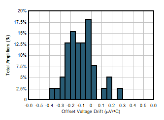
In precision data-acquisition applications, the OPAx210 provide fast settling time to 16-bit accuracy, even for 10-V output swings. Excellent ac performance, combined with only 35 μV (maximum) of offset and 0.6 µV/°C (maximum) drift over temperature, makes the OPAx210 an excellent choice for high-speed, high-precision applications.
The OPAx210 are specified over a wide dual power-supply range of ±2.25 V to ±18 V, or single-supply operation from 4.5 V to 36 V, are specified from –40°C to +125°C.
| PART NUMBER | PACKAGE(1) | BODY SIZE (NOM) |
|---|---|---|
| OPA210 | SOIC (8) | 2.90 mm × 1.60 mm |
| SOT-23 (5) | 2.90 mm × 1.60 mm | |
| VSSOP (8) | 3.00 mm × 3.00 mm | |
| OPA2210 | SOIC (8) | 4.90 mm × 3.91 mm |
| VSSOP (8) | 3.00 mm × 3.00 mm | |
| WSON (8) | 3.00 mm × 3.00 mm |
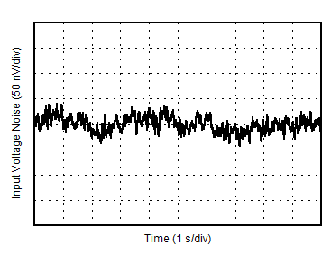
 OPAx210 0.1-Hz to
10-Hz Noise
 OPAx210 Offset
Voltage Drift Distribution