SBOS924H September 2018 – August 2021 OPA210 , OPA2210
PRODUCTION DATA
- 1 Features
- 2 Applications
- 3 Description
- 4 Revision History
- 5 Pin Configuration and Functions
- 6 Specifications
- 7 Detailed Description
- 8 Application and Implementation
- 9 Power Supply Recommendations
- 10Layout
- 11Device and Documentation Support
- 12Mechanical, Packaging, and Orderable Information
Package Options
Mechanical Data (Package|Pins)
Thermal pad, mechanical data (Package|Pins)
- DRG|8
Orderable Information
7.3.3 Noise Performance
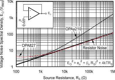
Figure 7-2 shows the total circuit noise for varying source impedances with the op amp in a unity-gain configuration (no feedback resistor network, and therefore, no additional noise contributions). Two different op amps are shown with the total circuit noise calculated. The OPAx210 have very low voltage noise, making these devices a great choice for low source impedances (less than 2 kΩ). As a comparable, precision FET-input op amp (very low current noise), the OPA827 has somewhat higher voltage noise, but lower current noise. The device provides excellent noise performance at moderate to high source impedance (10 kΩ and up). For source impedance lower than 300 Ω, the OPA211 may provide lower noise.
The equation in Figure 7-2 shows the calculation of the total circuit noise, with these parameters:
- en = voltage noise,
- in = current noise,
- RS = source impedance,
- k = Boltzmann's constant = 1.38 × 10⁻²³ J/K, and
- T = temperature in kelvins
For more details on calculating noise, see Section 8.1.1.
 Figure 7-2 Noise Performance
of the OPAx210 and OPA827 in Unity-Gain Buffer
Configuration