SBOS955 February 2019 OPA2356-EP
PRODUCTION DATA.
- 1 Features
- 2 Applications
- 3 Description
- 4 Revision History
- 5 Pin Configuration and Functions
- 6 Specifications
- 7 Detailed Description
- 8 Application and Implementation
- 9 Power Supply Recommendations
- 10Layout
- 11Device and Documentation Support
- 12Mechanical, Packaging, and Orderable Information
Package Options
Mechanical Data (Package|Pins)
- DGK|8
Thermal pad, mechanical data (Package|Pins)
- DGK|8
Orderable Information
8.2.3 Driving ADCs
The OPA2356-EP op amps are designed for driving sampling analog-to-digital converters (ADCs) with sampling speeds up to 1 MSPS. The zero-crossover distortion input stage topology allows the OPA2356-EP to drive ADCs without degradation of differential linearity and THD.
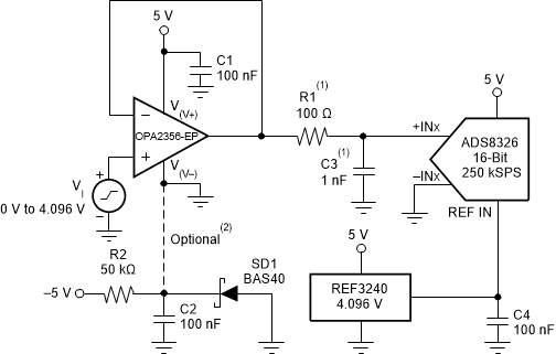
The OPA2356-EP can be used to buffer the ADC switched input capacitance and resulting charge injection while providing signal gain. Figure 34 shows the OPA2356-EP configured to drive the ADS8326.

1. Suggested value; may require adjustment based on specific application.
2. Single-supply applications lose a small number of ADC codes near ground as a result of op amp output swing limitation. If a negative power supply is available, this simple circuit creates a –0.3-V supply to allow output swing to true ground potential.
Figure 34. Driving the ADS8326