SBOS984G November 2020 – September 2023 OPA2387 , OPA387 , OPA4387
PRODUCTION DATA
- 1
- 1 Features
- 2 Applications
- 3 Description
- 4 Revision History
- 5 Pin Configuration and Functions
- 6 Specifications
- 7 Detailed Description
- 8 Application and Implementation
- 9 Device and Documentation Support
- 10Mechanical, Packaging, and Orderable Information
Package Options
Mechanical Data (Package|Pins)
Thermal pad, mechanical data (Package|Pins)
Orderable Information
3 Description
The OPA387, OPA2387, and OPA4387 (OPAx387) family of precision amplifiers offers state-of-the-art performance. With zero-drift technology, the OPAx387 offset voltage and offset drift provide unparalleled long-term stability. With a mere 570 µA of quiescent current, the OPAx387 are able to achieve 5.7 MHz of bandwidth, a broadband noise of 8.5 nV/√Hz, and a 1/f noise at 177 nVPP. These specifications are crucial to achieve extremely-high precision and no degradation of linearity in 16-bit to 24-bit analog to digital converters (ADCs). The OPAx387 feature flat bias current over temperature; therefore, little to no calibration is needed in high input impedance applications over temperature.
All versions are specified over the industrial temperature range of –40°C to +125°C.
| PART NUMBER | CHANNEL COUNT | PACKAGE(1) |
|---|---|---|
| OPA387 | Single | DBV (SOT-23, 5) |
| OPA2387 | Dual | D (SOIC, 8) |
| DGK (VSSOP, 8) | ||
| DSG (WSON, 8) | ||
| OPA4387 | Quad | PW (TSSOP, 14) |
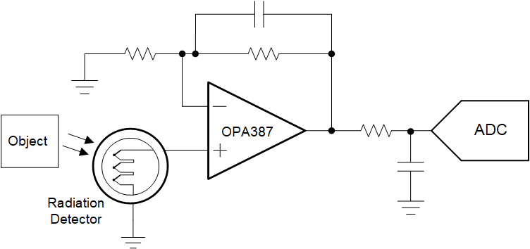
 The OPA387 as an
Ultra-Low Offset, Low-Noise ADC Driver
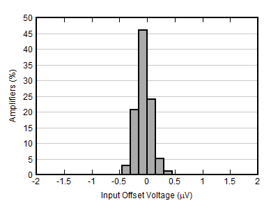
 Ultra-Low Input Offset Voltage