SBOSA38A February 2021 – April 2021 OPA2607-Q1 , OPA607-Q1
PRODUCTION DATA
- 1 Features
- 2 Applications
- 3 Description
- 4 Revision History
- 5 Device Comparison
- 6 Pin Configuration and Functions
- 7 Specifications
- 8 Detailed Description
- 9 Application and Implementation
- 10Power Supply Recommendations
- 11Layout
- 12Device and Documentation Support
- 13Mechanical, Packaging, and Orderable Information
Package Options
Mechanical Data (Package|Pins)
- DGK|8
Thermal pad, mechanical data (Package|Pins)
Orderable Information
8.3.2 Rail-to-Rail Output and Driving Capacitive Loads
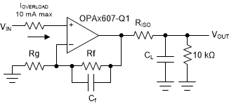
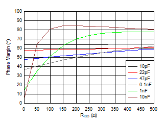
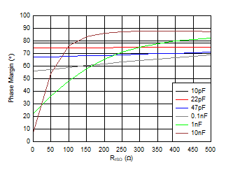
Designed as a low-power, low-voltage operational amplifier, the OPAx607-Q1 devices are capable of delivering a robust output drive. For resistive loads of 10 kΩ, the output swings to within a few millivolts of either supply rail, regardless of the applied power-supply voltage. Different load conditions change the ability of the amplifier to swing close to the rails. The OPAx607-Q1 devices drive up to a nominal capacitive load of 47 pF on the output with no special consideration and without the need of a series isolation resistor RISO while still being able to achieve 45° of phase margin. When driving capacitive loads greater than 47 pF, TI recommends using RISO as shown in Figure 8-1 in series with the output as close to the device as possible. Refer to Figure 7-18 for looking up different values of RISO required for CL to achieve 45° phase margin. Without RISO, the external capacitance (CL) interacts with the output impedance (ZO) of the amplifier, resulting in stability issues. Inserting RISO isolates CL from ZO and restores the phase margin. Figure 8-1 shows the test circuit.
 Figure 8-1 Input Current Protection and Driving Capacitive Loads
Figure 8-2 and Figure 8-3 show the phase margin achieved with varying RISO with different values of CL.

| Gain = 10 V/V, | Cf = 2.5 pF, | RL = 10 kΩ |

| Gain = 20 V/V, | Cf = 2.5 pF, | RL = 10 kΩ |