SBOS933I February 2019 – August 2021 OPA2990 , OPA4990 , OPA990
PRODUCTION DATA
- 1 Features
- 2 Applications
- 3 Description
- 4 Revision History
- 5 Pin Configuration and Functions
- 6 Specifications
-
7 Detailed Description
- 7.1 Overview
- 7.2 Functional Block Diagram
- 7.3
Feature Description
- 7.3.1 Input Protection Circuitry
- 7.3.2 EMI Rejection
- 7.3.3 Thermal Protection
- 7.3.4 Capacitive Load and Stability
- 7.3.5 Common-Mode Voltage Range
- 7.3.6 Phase Reversal Protection
- 7.3.7 Electrical Overstress
- 7.3.8 Overload Recovery
- 7.3.9 Typical Specifications and Distributions
- 7.3.10 Packages With an Exposed Thermal Pad
- 7.3.11 Shutdown
- 7.4 Device Functional Modes
- 8 Application and Implementation
- 9 Power Supply Recommendations
- 10Layout
- 11Device and Documentation Support
- 12Mechanical, Packaging, and Orderable Information
7.3.3 Thermal Protection
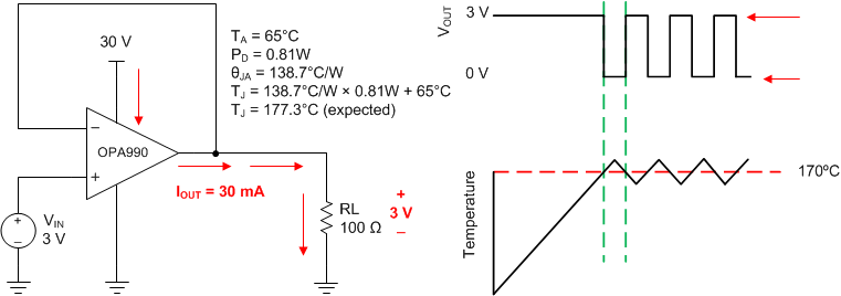
The internal power dissipation of any amplifier causes its internal (junction) temperature to rise. This phenomenon is called self heating. The absolute maximum junction temperature of the OPAx990 is 150°C. Exceeding this temperature causes damage to the device. The OPAx990 has a thermal protection feature that reduces damage from self heating. The protection works by monitoring the temperature of the device and turning off the op amp output drive for temperatures above 170°C. Figure 7-4 shows an application example for the OPA990 that has significant self heating because of its power dissipation (0.81 W). Thermal calculations indicate that for an ambient temperature of 65°C, the device junction temperature must reach 177°C. The actual device, however, turns off the output drive to recover towards a safe junction temperature. Figure 7-4 shows how the circuit behaves during thermal protection. During normal operation, the device acts as a buffer so the output is 3 V. When self heating causes the device junction temperature to increase above the internal limit, the thermal protection forces the output to a high-impedance state and the output is pulled to ground through resistor RL. If the condition that caused excessive power dissipation is not removed, the amplifier will oscillate between a shutdown and enabled state until the output fault is corrected.
 Figure 7-4 Thermal Protection