SBOS110C May 1998 – March 2023 OPA2227 , OPA2228 , OPA227 , OPA228 , OPA4227 , OPA4228
PRODUCTION DATA
- 1 Features
- 2 Applications
- 3 Description
- 4 Revision History
- 5 Pin Configuration and Functions
-
6 Specifications
- 6.1 Absolute Maximum Ratings
- 6.2 ESD Ratings
- 6.3 Recommended Operating Conditions
- 6.4 Thermal Information: OPA227, OPA228
- 6.5 Thermal Information: OPA2227, OPA2228
- 6.6 Thermal Information: OPA4227, OPA4228
- 6.7 Electrical Characteristics: OPAx227
- 6.8 Electrical Characteristics: OPAx228
- 6.9 Typical Characteristics
- 7 Detailed Description
-
8 Application and Implementation
- 8.1 Application Information
- 8.2 Typical Application
- 8.3 Power Supply Recommendations
- 8.4 Layout
- 9 Device and Documentation Support
- 10Mechanical, Packaging, and Orderable Information
Package Options
Mechanical Data (Package|Pins)
Thermal pad, mechanical data (Package|Pins)
Orderable Information
7.3.5 Input Bias Current Cancellation
The input bias current of the OPAx22x series is internally compensated with an equal and opposite cancellation current. The resulting input bias current is the difference between with input bias current and the cancellation current. The residual input bias current can be positive or negative.
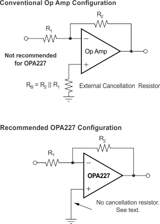
When the bias current is canceled in this manner, the input bias current and input offset current are approximately equal. A resistor added to cancel the effect of the input bias current (as shown in Figure 7-3) can actually increase offset and noise and is therefore not recommended.
 Figure 7-3 Input Bias Current Cancellation