SBOS110C May 1998 – March 2023 OPA2227 , OPA2228 , OPA227 , OPA228 , OPA4227 , OPA4228
PRODUCTION DATA
- 1 Features
- 2 Applications
- 3 Description
- 4 Revision History
- 5 Pin Configuration and Functions
-
6 Specifications
- 6.1 Absolute Maximum Ratings
- 6.2 ESD Ratings
- 6.3 Recommended Operating Conditions
- 6.4 Thermal Information: OPA227, OPA228
- 6.5 Thermal Information: OPA2227, OPA2228
- 6.6 Thermal Information: OPA4227, OPA4228
- 6.7 Electrical Characteristics: OPAx227
- 6.8 Electrical Characteristics: OPAx228
- 6.9 Typical Characteristics
- 7 Detailed Description
-
8 Application and Implementation
- 8.1 Application Information
- 8.2 Typical Application
- 8.3 Power Supply Recommendations
- 8.4 Layout
- 9 Device and Documentation Support
- 10Mechanical, Packaging, and Orderable Information
Package Options
Mechanical Data (Package|Pins)
Thermal pad, mechanical data (Package|Pins)
Orderable Information
7.3.6 Noise Performance
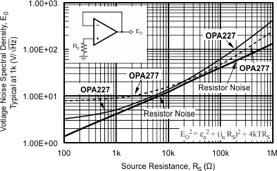
Figure 7-4 shows the total circuit noise for varying source impedances with the operational amplifier in a unity-gain configuration (no feedback resistor network; therefore, no additional noise contributions). Two different operational amplifiers are shown with total circuit noise calculated. The OPA227 has very low voltage noise, making this device an excellent choice for low source impedances (less than 20 kΩ). A similar precision operational amplifier, the OPA277, has somewhat higher voltage noise but lower current noise. The OPA277 provides excellent noise performance at moderate source impedance (10 kΩ to 100 kΩ). Above 100 kΩ, a FET-input operational amplifier such as the OPA132 (very low current noise) can provide improved performance. Use the equation in Figure 7-4 to calculate the total circuit noise, where en = voltage noise, in = current noise, RS = source impedance, k = Boltzmann’s constant = 1.38 × 10⁻²³ J/K, and T is temperature in K. For more details on calculating noise, see Section 7.3.7.
 Figure 7-4 Noise
Performance of the OPA227 in Unity-Gain Buffer Configuration