SBOS110C May 1998 – March 2023 OPA2227 , OPA2228 , OPA227 , OPA228 , OPA4227 , OPA4228
PRODUCTION DATA
- 1 Features
- 2 Applications
- 3 Description
- 4 Revision History
- 5 Pin Configuration and Functions
-
6 Specifications
- 6.1 Absolute Maximum Ratings
- 6.2 ESD Ratings
- 6.3 Recommended Operating Conditions
- 6.4 Thermal Information: OPA227, OPA228
- 6.5 Thermal Information: OPA2227, OPA2228
- 6.6 Thermal Information: OPA4227, OPA4228
- 6.7 Electrical Characteristics: OPAx227
- 6.8 Electrical Characteristics: OPAx228
- 6.9 Typical Characteristics
- 7 Detailed Description
-
8 Application and Implementation
- 8.1 Application Information
- 8.2 Typical Application
- 8.3 Power Supply Recommendations
- 8.4 Layout
- 9 Device and Documentation Support
- 10Mechanical, Packaging, and Orderable Information
Package Options
Mechanical Data (Package|Pins)
Thermal pad, mechanical data (Package|Pins)
- D|14
Orderable Information
5 Pin Configuration and Functions
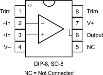
 Figure 5-1 OPA227, OPA228: D (8-Pin
SOIC) or P (8-Pin PDIP) Package (Top View)
Figure 5-1 OPA227, OPA228: D (8-Pin
SOIC) or P (8-Pin PDIP) Package (Top View)Table 5-1 Pin Functions: OPA227 and OPA228
| PIN | TYPE | DESCRIPTION | ||
|---|---|---|---|---|
| NO. | NAME | |||
| 1 | Offset Trim | Input | Input offset voltage trim (leave floating if not used) | |
| 2 | -In | Input | Inverting input | |
| 3 | +In | Input | Noninverting input | |
| 4 | V- | — | Negative (lowest) power supply | |
| 5 | NC | — | No internal connection (can be left floating) | |
| 6 | Output | Output | Output | |
| 7 | V+ | — | Positive (highest) power supply | |
| 8 | Trim | — | Input offset voltage trim (leave floating if not used) | |
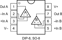
 Figure 5-2 OPA2227, OPA2228: D (8-Pin SOIC) or P (8-Pin PDIP) Package (Top
View)
Figure 5-2 OPA2227, OPA2228: D (8-Pin SOIC) or P (8-Pin PDIP) Package (Top
View)Table 5-2 Pin Functions: OPA2227 and OPA2228
| PIN | TYPE | DESCRIPTION | |
|---|---|---|---|
| NO. | NAME | ||
| 1 | Out A | Output | Output channel A |
| 2 | –In A | Input | Inverting input channel A |
| 3 | +In A | Input | Noninverting input channel A |
| 4 | V- | — | Negative (lowest) power supply |
| 5 | +In B | Input | Noninverting input channel B |
| 6 | –In B | Input | Inverting input channel B |
| 7 | Out B | Output | Output channel B |
| 8 | V+ | — | Positive (highest) power supply |
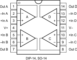
 Figure 5-3 OPA4227, OPA4228: D (14-Pin SOIC) or N
(14-Pin PDIP) Package (Top View)
Figure 5-3 OPA4227, OPA4228: D (14-Pin SOIC) or N
(14-Pin PDIP) Package (Top View)Table 5-3 Pin Functions: OPA4227 and OPA4228
| PIN | TYPE | DESCRIPTION | ||
|---|---|---|---|---|
| NO. | NAME | |||
| 1 | Out A | Output | Output channel A | |
| 2 | -In A | Input | Inverting input channel A | |
| 3 | +In A | Input | Noninverting input channel A | |
| 4 | V+ | — | Positive (highest) power supply | |
| 5 | +In B | Input | Noninverting input channel B | |
| 6 | -In B | Input | Inverting input channel B | |
| 7 | Out B | Output | Output channel B | |
| 8 | Out C | Output | Output channel C | |
| 9 | -In C | Input | Inverting input channel C | |
| 10 | +In C | Input | Noninverting input channel C | |
| 11 | V- | — | Negative (lowest) power supply | |
| 12 | +In D | Input | Noninverting input channel D | |
| 13 | -In D | Input | Inverting input channel D | |
| 14 | Out D | Output | Output channel D | |