SLOSEE7 May   2025 OPA810-Q1

PRODUCTION DATA  

  1.   1
  2. Features
  3. Applications
  4. Description
  5. Device Comparison Table
  6. Pin Configuration and Functions
  7. Specifications
    1. 6.1 Absolute Maximum Ratings
    2. 6.2 ESD Ratings
    3. 6.3 Recommended Operating Conditions
    4. 6.4 Thermal Information
    5. 6.5 Electrical Characteristics: 24V
    6. 6.6 Electrical Characteristics: 5V
    7. 6.7 Typical Characteristics: VS = 24V
    8. 6.8 Typical Characteristics: VS = 5V
    9. 6.9 Typical Characteristics: ±2.375V to ±12V Split Supply
  8. Detailed Description
    1. 7.1 Overview
    2. 7.2 Functional Block Diagram
    3. 7.3 Feature Description
      1. 7.3.1 Architecture
      2. 7.3.2 ESD Protection
    4. 7.4 Device Functional Modes
      1. 7.4.1 Split-Supply Operation (±2.375V to ±13.5V)
      2. 7.4.2 Single-Supply Operation (4.75V to 27V)
  9. Application and Implementation
    1. 8.1 Application Information
      1. 8.1.1 Amplifier Gain Configurations
      2. 8.1.2 Selection of Feedback Resistors
      3. 8.1.3 Noise Analysis and the Effect of Resistor Elements on Total Noise
    2. 8.2 Typical Applications
      1. 8.2.1 Transimpedance Amplifier
        1. 8.2.1.1 Design Requirements
        2. 8.2.1.2 Detailed Design Procedure
        3. 8.2.1.3 Application Curves
      2. 8.2.2 Multichannel Sensor Interface
    3. 8.3 Power Supply Recommendations
    4. 8.4 Layout
      1. 8.4.1 Layout Guidelines
        1. 8.4.1.1 Thermal Considerations
      2. 8.4.2 Layout Example
  10. Device and Documentation Support
    1. 9.1 Documentation Support
      1. 9.1.1 Related Documentation
    2. 9.2 Receiving Notification of Documentation Updates
    3. 9.3 Support Resources
    4. 9.4 Trademarks
    5. 9.5 Electrostatic Discharge Caution
    6. 9.6 Glossary
  11. 10Revision History
  12. 11Mechanical, Packaging, and Orderable Information

Package Options

Refer to the PDF data sheet for device specific package drawings

Mechanical Data (Package|Pins)
  • DBV|5
Thermal pad, mechanical data (Package|Pins)
Orderable Information

Typical Characteristics: VS = 5V

at VS+ = 5V, VS– = 0V, VCM= 1.25V, RL = 1kΩ, output is biased to midsupply, and TA ≅ 25°C; for ac specifications, VS+ = 3.5V, VS– = –1.5V, VCM = 0V, VO = 2VPP, gain (G) = 2V/V, RF = 1kΩ, and CL = 4.7pF (unless otherwise noted)

OPA810-Q1 Small-Signal
            Response vs Gain
See Figure 8-1 and Figure 8-2, VO = 20mVPP
Figure 6-17 Small-Signal Response vs Gain
OPA810-Q1 Overshoot and
            Undershoot vs CL
See Figure 8-1, G = 1V/V, RF = 0Ω
Figure 6-19 Overshoot and Undershoot vs CL
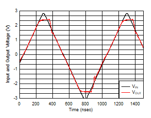
OPA810-Q1 Output
            Overdrive Recovery
See Figure 8-2, G = –1V/V
Figure 6-21 Output Overdrive Recovery
OPA810-Q1 Output
            Short-Circuit Current vs Ambient Temperature
Output saturated and then short-circuited
Figure 6-23 Output Short-Circuit Current vs Ambient Temperature
OPA810-Q1 Small-Signal
            Transient Response
See Figure 8-1, G = 1V/V, RF = 0Ω, CL = 10pF
Figure 6-18 Small-Signal Transient Response
OPA810-Q1 Input Overdrive
            Recovery
See Figure 8-1, G = 1V/V, RF = 0Ω
Figure 6-20 Input Overdrive Recovery
OPA810-Q1 Output Voltage
            Range vs Output Current
 
Figure 6-22 Output Voltage Range vs Output Current
OPA810-Q1 Input Offset
            Voltage vs Input Common-Mode Voltage
Measured for 12 units
Figure 6-24 Input Offset Voltage vs Input Common-Mode Voltage