SBOS303D June 2004 – December 2016 OPA820
PRODUCTION DATA.
- 1 Features
- 2 Applications
- 3 Description
- 4 Revision History
- 5 Device Comparison Table
- 6 Pin Configuration and Functions
- 7 Specifications
- 8 Parameter Measurement Information
- 9 Detailed Description
- 10Application and Implementation
- 11Power Supply Recommendations
- 12Layout
- 13Device and Documentation Support
- 14Mechanical, Packaging, and Orderable Information
Package Options
Refer to the PDF data sheet for device specific package drawings
Mechanical Data (Package|Pins)
- D|8
- DBV|5
Thermal pad, mechanical data (Package|Pins)
Orderable Information
9 Detailed Description
9.1 Overview
The OPA820 provides an exceptional combination of DC precision, wide bandwidth, and low noise while consuming 5.6 mA of quiescent current. With excellent performance extending from DC to high frequencies, the OPA820 can be used in a variety of applications ranging from driving the inputs of high-precision SAR ADCs to video distributions systems.
9.2 Feature Description
9.2.1 Input and ESD Protection
The OPA820 device is built using a very high-speed complementary bipolar process. The internal junction breakdown voltages are relatively low for these very small geometry devices. These breakdowns are reflected in Absolute Maximum Ratings. All device pins are protected with internal ESD-protection diodes to the power supplies, as shown in Figure 52.
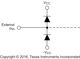 Figure 52. Internal ESD Protection
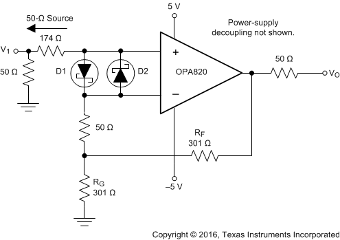
These diodes provide moderate protection to input overdrive voltages above the supplies as well. The protection diodes can typically support 30-mA continuous current. Where higher currents are possible (for example, in systems with ±15-V supply parts driving into the OPA820 device), add current-limiting series resistors into the two inputs. Keep these resistor values as low as possible because high values degrade both noise performance and frequency response. Figure 53 shows an example protection circuit for I/O voltages that may exceed the supplies.
9.2.2 Bandwidth versus Gain
Voltage-feedback op amps exhibit decreasing closed-loop bandwidth as the signal gain is increased. In theory, this relationship is described by the GBP listed in Specifications. Ideally, dividing GBP by the noninverting signal gain (also called the noise gain, or NG) predicts the closed-loop bandwidth. In practice, this prediction only holds true when the phase margin approaches 90°, as it does in high-gain configurations. At low signal gains, most amplifiers exhibit a more complex response with lower phase margin. The OPA820 device is optimized to give a maximally-flat, 2nd-order Butterworth response in a gain of 2. In this configuration, the OPA820 device has approximately 64° of phase margin and shows a typical –3-dB bandwidth of 240 MHz. When the phase margin is 64°, the closed-loop bandwidth is approximately √2 greater than the value predicted by dividing GBP by the noise gain.
Increasing the gain causes the phase margin to approach 90° and the bandwidth to more closely approach the predicted value of GBP / NG. At a gain of 10, the 30-MHz bandwidth shown in Electrical Characteristics: VS = ±5 V matches the prediction of the simple formula using the typical GBP of 280 MHz.
9.2.3 Output Drive Capability
The OPA820 device has been optimized to drive the demanding load of a doubly-terminated transmission line. When a 50-Ω line is driven, a series 50-Ω source resistor leading into the cable and a terminating 50-Ω load resistor at the end of the cable are used. Under these conditions, the cable impedance seems resistive over a wide frequency range, and the total effective load on the OPA820 device is 100 Ω in parallel with the resistance of the feedback network. Specifications lists a ±3.6-V swing into this load—which is then reduced to a ±1.8-V swing at the termination resistor. The ±75-mA output drive over temperature provides adequate current-drive margin for this load. Higher voltage swings (and lower distortion) are achievable when driving higher impedance loads.
A single video load typically appears as a 150-Ω load (using standard 75-Ω cables) to the driving amplifier. The OPA820 device provides adequate voltage and current drive to support up to three parallel video loads (50-Ω total load) for an NTSC signal. With only one load, the OPA820 device achieves an exceptionally low 0.01% or 0.03° dG/dP error.
9.2.4 Driving Capacitive Loads
One of the most demanding, and yet very common, load conditions for an op amp is capacitive loading. A high-speed, high open-loop gain amplifier like the OPA820 device can be very susceptible to decreased stability and closed-loop response peaking when a capacitive load is placed directly on the output pin. In simple terms, the capacitive load reacts with the open-loop output resistance of the amplifier to introduce an additional pole into the loop and thereby decrease the phase margin. This issue has become a popular topic of application notes and articles, and several external solutions to this problem have been suggested. When the primary considerations are frequency response flatness, pulse response fidelity, distortion, or a combination, the simplest and most effective solution is to isolate the capacitive load from the feedback loop by inserting a series isolation resistor between the amplifier output and the capacitive load. This solution does not eliminate the pole from the loop response, but rather shifts it and adds a zero at a higher frequency. The additional zero acts to cancel the phase lag from the capacitive load pole, thus increasing the phase margin and improving stability.
Figure 15 (±5 V) and Figure 42 (5 V) show the recommended RS versus capacitive load and the resulting frequency response at the load. The criterion for setting the recommended resistor is the maximum-bandwidth, flat-frequency response at the load. Because a passive low-pass filter is now between the output pin and the load capacitance, the response at the output pin is typically somewhat peaked, and becomes flat after the roll-off action of the RC network. This response is not a concern in most applications, but can cause clipping if the desired signal swing at the load is very close to the swing limit of the amplifier. Such clipping most likely to occurs in pulse response applications where the frequency peaking is manifested as an overshoot in the step response.
Parasitic capacitive loads greater than 2 pF can begin to degrade the performance of the OPA820 device. Long printed-circuit board traces, unmatched cables, and connections to multiple devices can easily cause this value to be exceeded. Always consider this effect carefully, and add the recommended series resistor as close as possible to the OPA820 output pin (see Layout Guidelines).
9.2.5 Distortion Performance
The OPA820 device is capable of delivering an exceptionally-low distortion signal at high frequencies and low gains. The distortion plots in Typical Characteristics show the typical distortion under a wide variety of conditions. Most of these plots are limited to 100-dB dynamic range. The OPA820 distortion does not rise above –90 dBc until either the signal level exceeds 0.9 V, the fundamental frequency exceeds 500 kHz, or both occur. Distortion in the audio band is less than or equal to –100 dBc.
Generally, until the fundamental signal reaches very high frequencies or powers, the 2nd-harmonic dominates the distortion with a negligible 3rd-harmonic component. Focusing then on the 2nd-harmonic, increasing the load impedance improves distortion directly. Remember that the total load includes the feedback network—in the noninverting configuration this is the sum of RF + RG, whereas in the inverting configuration this is just RF (see Figure 55). Increasing the output voltage swing directly increases harmonic distortion. Increasing the signal gain also increases the 2nd-harmonic distortion. Again, a 6-dB increase in gain increases the 2nd and 3rd-harmonic by 6 dB even with a constant output power and frequency. Finally, the distortion increases as the fundamental frequency increases because of the roll-off in the loop gain with frequency. Conversely, the distortion improves going to lower frequencies down to the dominant open-loop pole at approximately 100 kHz. Starting from the –85-dBc 2nd-harmonic for 2 VPP into 200 Ω, G = 2 distortion at 1 MHz (from Typical Characteristics), the 2nd-harmonic distortion does not show any improvement below 100 kHz and then becomes Equation 1.
9.2.6 Noise Performance
The OPA820 device complements low harmonic distortion with low input-noise terms. Both the input-referred voltage noise and the two input-referred current noise terms combine to give a low output noise under a wide variety of operating conditions. Figure 54 shows the op amp noise analysis model with all the noise terms included. In this model, all the noise terms are taken to be noise voltage or current density terms in either nV/√Hz or pA/√Hz.
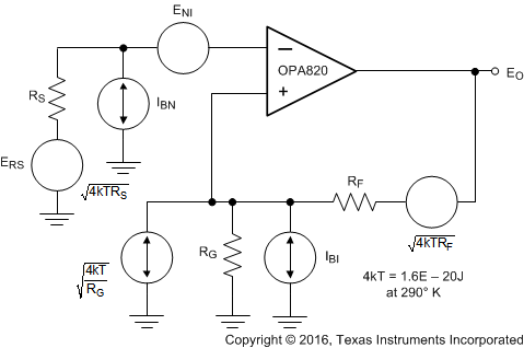 Figure 54. Op Amp Noise Analysis Model
The total output spot noise voltage is computed as the square root of the squared contributing terms to the output noise voltage. This computation is adding all the contributing noise powers at the output by superposition, then taking the square root to get back to a spot noise voltage. Equation 2 shows the general form for this output noise voltage using the terms presented in Figure 54.

Dividing this expression by the noise gain (NG = 1 + RF / RG) gives the equivalent input referred spot noise voltage at the noninverting input, as shown in Equation 3.

Evaluating these two equations for the OPA820 circuit shown in Figure 55 gives a total output spot noise voltage of 6.44 nV/√Hz and an equivalent input spot noise voltage of 3.22 nV/√Hz.
9.2.7 DC Offset Control
The OPA820 device can provide excellent DC-signal accuracy because of high open-loop gain, high common-mode rejection, high power-supply rejection, low input-offset voltage, and low bias-current offset errors. To take full advantage of this low input-offset voltage, careful attention to input bias-current cancellation is also required. The high-speed input stage for the OPA820 device has a moderately high input bias current (9 µA typical into the pins) but with a very close match between the two input currents—typically 100-nA input offset current. The total output-offset voltage can be considerably reduced by matching the source impedances looking out of the two inputs. For example, one way to add bias current cancellation to the circuit of Figure 55 is to insert a 175-Ω series resistor into the noninverting input from the 50-Ω terminating resistor. When the 50-Ω source resistor is DC-coupled, the source impedance for the noninverting input bias current increases to 200 Ω. Because this value is now equal to the impedance looking out of the inverting input (RF || RG), the circuit cancels the gains for the bias currents to the output leaving only the offset current times the feedback resistor as a residual DC error term at the output. Using a 402-Ω feedback resistor, this output error is now less than ±0.4 µA × 402 Ω = ±160 µV at 25°C.
9.2.8 Thermal Analysis
The OPA820 device does not require heat sinking or airflow in most applications. The maximum desired junction temperature sets the maximum allowed internal power dissipation as described in this section. Make sure that the maximum junction temperature does not exceed 150°C.
Use Equation 4 to calculate the operating junction temperature (TJ).
The total internal power dissipation (PD) is the sum of quiescent power (PDQ) and additional power dissipated in the output stage (PDL) to deliver load power. Quiescent power is the specified no-load supply current times the total supply voltage across the part. PDL depends on the required output signal and load but, for a grounded resistive load, is at a maximum when the output is fixed at a voltage equal to ½ of either supply voltage (for equal bipolar supplies). Under this worst-case condition, use Equation 5 to calculate PDL.
where
- RL includes feedback network loading.
NOTE
The power in the output stage and not in the load that determines internal power
dissipation.
As a worst-case example, compute the maximum TJ using an OPA820IDBV (SOT23-5 package) in the circuit of Figure 55 operating at the maximum specified ambient temperature of 85°C.
9.3 Device Functional Modes
9.3.1 Wideband Noninverting Operation
The combination of speed and dynamic range offered by the OPA820 device is easily achieved in a wide variety of application circuits, providing that simple principles of good design practice are observed. For example, good power-supply decoupling, as shown in Figure 55, is essential to achieve the lowest-possible harmonic distortion and smooth frequency response.
Proper PCB layout and careful component selection maximize the performance of the OPA820 device in all applications, as discussed in the following sections of this data sheet.
Figure 55 shows the gain of 2 configuration used as the basis for most of the typical characteristics. Most of the curves in Typical Characteristics were characterized using signal sources with a 50-Ω driving impedance and with measurement equipment presenting 50-Ω load impedance. In Figure 55, the 50-Ω shunt resistor at the VI terminal matches the source impedance of the test generator while, the 50-Ω series resistor at the VO terminal provides a matching resistor for the measurement equipment load. Generally, data sheet specifications refer to the voltage swings at the output pin (VO in Figure 55). The 100-Ω load, combined with the 804-Ω total feedback network load, presents the OPA820 device with an effective load of approximately 90 Ω in Figure 55.
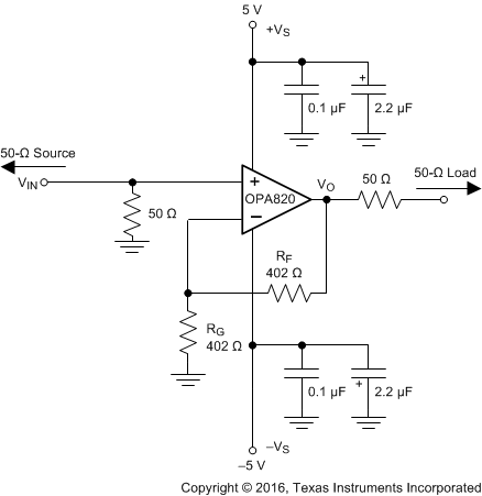 Figure 55. Gain of 2, High-Frequency Application and Characterization Circuit
9.3.2 Wideband Inverting Operation
Operating the OPA820 device as an inverting amplifier has several benefits and is particularly useful when a matched 50-Ω source and input impedance is required. Figure 56 shows the inverting gain of –1 circuit used as the basis of the inverting mode curves in Typical Characteristics.
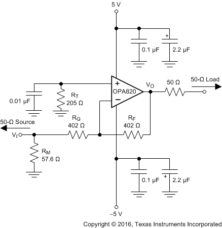 Figure 56. Inverting G = –1 Specifications and Test Circuit
In the inverting case, only the feedback resistor appears as part of the total output load in parallel with the actual load. For the 100-Ω load used in the curves in Typical Characteristics, this results in a total load of 80 Ω in this inverting configuration. The gain resistor is set to get the desired gain (in this case 402 Ω for a gain of –1) while an additional input-matching resistor (RM) can be used to set the total input impedance equal to the source if desired. In this case, RM is 57.6 Ω in parallel with the 402-Ω gain setting resistor results in a matched input impedance of 50 Ω. This matching is only required when the input must be matched to a source impedance, as in the characterization testing done using the circuit of Figure 56.
The OPA820 device offers extremely good DC accuracy as well as low noise and distortion. To take full advantage of that DC precision, the total DC impedance at each of the input nodes must be matched to get bias current cancellation. For the circuit of Figure 56, this matching requires the 205-Ω resistor to ground on the noninverting input. The calculation for this resistor includes a DC-coupled 50-Ω source impedance along with RG and RM. Although this resistor provides cancellation for the bias current, it must be well decoupled (0.01 µF in Figure 56) to filter the noise contribution of the resistor and the input current noise.
As the required RG resistor approaches 50 Ω at higher gains, the bandwidth for the circuit in Figure 56 exceeds the bandwidth at that same gain magnitude for the noninverting circuit of Figure 55 which occurs because of the lower noise gain for the circuit of Figure 56 when the 50-Ω source impedance is included in the analysis. For instance, at a signal gain of –10 (RG = 50 Ω, RM = open, RF = 499 Ω) the noise gain for the circuit of Figure 56 is shown in Equation 8.
Equation 8 is a result of adding the 50-Ω source in the noise gain equation which results in a considerably higher bandwidth than the noninverting gain of 10. Using the 240-MHz gain bandwidth product for the OPA820 device, an inverting gain of –10 from a 50-Ω source to a 50-Ω RG gives 55-MHz bandwidth, whereas the noninverting gain of 10 gives 30 MHz.
9.3.3 Wideband Single-Supply Operation
Figure 57 shows the AC-coupled, single 5-V supply, gain of 2-V/V circuit configuration used as a basis only for the 5-V specifications in Specifications. The most important requirement for single-supply operation is to maintain input and output-signal swings within the useable voltage ranges at both the input and the output. The circuit of Figure 57 establishes an input midpoint bias using a simple resistive divider from the 5-V supply (two 806-Ω resistors) to the noninverting input. The input signal is then AC-coupled into this midpoint voltage bias. The input voltage can swing to within 0.9 V of the negative supply and 0.5 V of the positive supply, giving a 3.6-VPP input-signal range. The input impedance-matching resistor (57.6 Ω) used in Figure 57 is adjusted to give a 50-Ω input match when the parallel combination of the biasing divider network is included. The gain resistor (RG) is AC-coupled, giving the circuit a DC gain of 1 which puts the input DC bias voltage (2.5 V) on the output as well. On a single 5-V supply, the output voltage can swing to within 1.3 V of either supply pin while delivering more than 80-mA output current giving 2.4-V output swing into 100 Ω (5.6 dBm maximum at the matched load).
Figure 58 shows the AC-coupled, single 5-V supply, gain of –1-V/V circuit configuration used as a basis only for the 5-V specifications in Specifications. In this case, the midpoint DC bias on the noninverting input is also decoupled with an additional 0.01-µF decoupling capacitor which reduces the source impedance at higher frequencies for the noninverting-input bias-current noise. This 2.5-V bias on the noninverting input pin appears on the inverting input pin and, because RG is DC blocked by the input capacitor, also appears at the output pin.
The single-supply test circuits of Figure 57 and Figure 58 show 5-V operation. These same circuits can be used with a single-supply of 5 V to 12 V. Operating on a single 12-V supply, with the absolute-maximum supply-voltage specification of 13 V, gives adequate design margin for the typical ±5% supply tolerance.
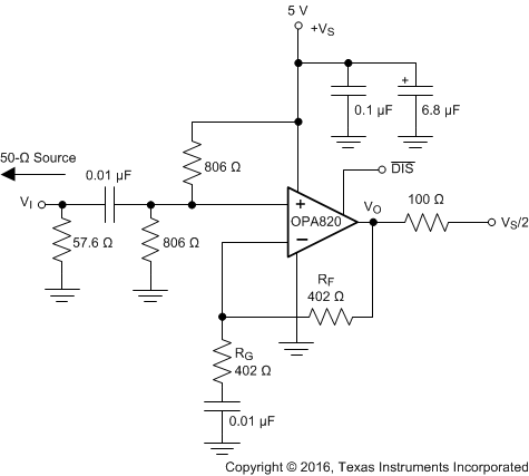 Figure 57. AC-Coupled, G = 2 V/V, Single-Supply Specifications and Test Circuit
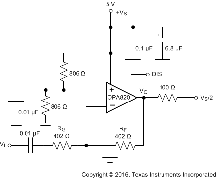 Figure 58. AC-Coupled, G = –1 V/V, Single-Supply Specifications and Test Circuit