SBOS303D June   2004  – December 2016 OPA820

PRODUCTION DATA.  

  1. Features
  2. Applications
  3. Description
  4. Revision History
  5. Device Comparison Table
  6. Pin Configuration and Functions
  7. Specifications
    1. 7.1 Absolute Maximum Ratings
    2. 7.2 ESD Ratings
    3. 7.3 Recommended Operating Conditions
    4. 7.4 Thermal Information
    5. 7.5 Electrical Characteristics: VS = ±5 V
    6. 7.6 Electrical Characteristics: VS = 5 V
    7. 7.7 Typical Characteristics
      1. 7.7.1 ±5-V Supply Voltage
      2. 7.7.2 5-V Supply Voltage
  8. Parameter Measurement Information
  9. Detailed Description
    1. 9.1 Overview
    2. 9.2 Feature Description
      1. 9.2.1 Input and ESD Protection
      2. 9.2.2 Bandwidth versus Gain
      3. 9.2.3 Output Drive Capability
      4. 9.2.4 Driving Capacitive Loads
      5. 9.2.5 Distortion Performance
      6. 9.2.6 Noise Performance
      7. 9.2.7 DC Offset Control
      8. 9.2.8 Thermal Analysis
    3. 9.3 Device Functional Modes
      1. 9.3.1 Wideband Noninverting Operation
      2. 9.3.2 Wideband Inverting Operation
      3. 9.3.3 Wideband Single-Supply Operation
  10. 10Application and Implementation
    1. 10.1 Application Information
      1. 10.1.1 Optimizing Resistor Values
    2. 10.2 Typical Applications
      1. 10.2.1 Active Filter Design
        1. 10.2.1.1 Design Requirements
        2. 10.2.1.2 Detailed Design Procedure
          1. 10.2.1.2.1 High-Q Bandpass Filter Design Procedure
          2. 10.2.1.2.2 Low-Pass Butterworth Filter Design Procedure
        3. 10.2.1.3 Application Curves
      2. 10.2.2 Buffering High-Performance ADCs
      3. 10.2.3 Video Line Driving
      4. 10.2.4 Single Differential Op Amp
      5. 10.2.5 Triple Differencing Op Amp (Instrumentation Topology)
      6. 10.2.6 DAC Transimpedance Amplifier
  11. 11Power Supply Recommendations
  12. 12Layout
    1. 12.1 Layout Guidelines
      1. 12.1.1 Minimizing Parasitic Capacitance
      2. 12.1.2 Minimizing Distance from Power Supply to Decoupling Capacitors
      3. 12.1.3 Selecting and Placing External Components
      4. 12.1.4 Connecting Other Wideband Devices
      5. 12.1.5 Socketing
    2. 12.2 Layout Example
  13. 13Device and Documentation Support
    1. 13.1 Device Support
      1. 13.1.1 Design-In Tools
        1. 13.1.1.1 Demonstration Fixtures
        2. 13.1.1.2 Macromodels and Applications Support
      2. 13.1.2 Development Support
    2. 13.2 Documentation Support
      1. 13.2.1 Related Documentation
    3. 13.3 Receiving Notification of Documentation Updates
    4. 13.4 Community Resources
    5. 13.5 Trademarks
    6. 13.6 Electrostatic Discharge Caution
    7. 13.7 Glossary
  14. 14Mechanical, Packaging, and Orderable Information

Package Options

Refer to the PDF data sheet for device specific package drawings

Mechanical Data (Package|Pins)
  • D|8
  • DBV|5
Thermal pad, mechanical data (Package|Pins)
Orderable Information

Parameter Measurement Information

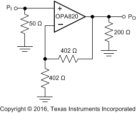
OPA820 pmi_p-m5v_two-tone_sbos303.gif Figure 48. Circuit for ±5-V Two-Tone, 3rd-Order Intermodulation Intercept (Figure 14)
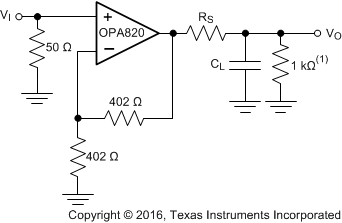
OPA820 pmi_p-m5v_freq-response_sbos303.gif
1 kΩ is optional.
Figure 49. Circuit for ±5-V Frequency Response vs Capacitive Load (Figure 55)
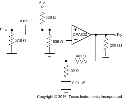
OPA820 pmi_5v_two-tone_sbos303.gif Figure 50. Circuit for 5-V Two-Tone, 3rd-Order Intermodulation Intercept (Figure 41)
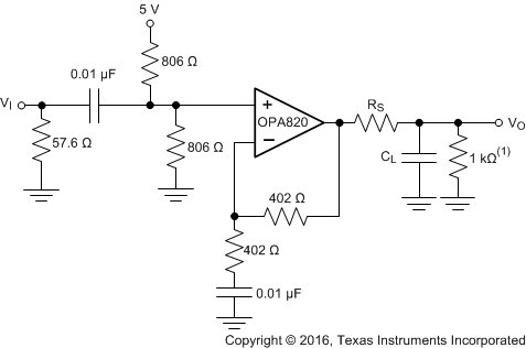
OPA820 pmi_5v_freq-response_sbos303.gif
This resistor is optional.
Figure 51. Circuit for 5-V Frequency Response vs Capacitive Load (Figure 43)