SLAS831D March   2014  – March 2018 PCM1860 , PCM1861 , PCM1862 , PCM1863 , PCM1864 , PCM1865

PRODUCTION DATA.  

  1. Features
  2. Applications
  3. Description
    1.     Device Images
      1.      Simplified Application Diagram
  4. Revision History
  5. Device Comparison Table
  6. Pin Configuration and Functions
    1.     Pin Functions: PCM1860 and PCM1861
    2.     Pin Functions: PCM1862, PCM1863, PCM1864, and PCM1865
  7. Specifications
    1. 7.1  Absolute Maximum Ratings
    2. 7.2  ESD Ratings
    3. 7.3  Recommended Operating Conditions
    4. 7.4  Thermal Information
    5. 7.5  Electrical Characteristics: PGA and ADC AC Performance
    6. 7.6  Electrical Characteristics: DC
    7. 7.7  Electrical Characteristics: Digital Filter
    8. 7.8  Timing Requirements: External Clock
    9. 7.9  Timing Requirements: I2C Control Interface
    10. 7.10 Timing Requirements: SPI Control Interface
    11. 7.11 Timing Requirements: Audio Data Interface for Slave Mode
    12. 7.12 Timing Requirements: Audio Data Interface for Master Mode
    13. 7.13 Typical Characteristics
  8. Parameter Measurement Information
  9. Detailed Description
    1. 9.1 Overview
    2. 9.2 Functional Block Diagrams
    3. 9.3 Features Description
      1. 9.3.1  Analog Front End
      2. 9.3.2  Microphone Support
        1. 9.3.2.1 Mic Bias
      3. 9.3.3  Input Multiplexer (PCM1860 and PCM1861)
      4. 9.3.4  Mixers and Multiplexers (PCM1862, PCM1863, PCM1864, and PCM1865)
      5. 9.3.5  Programmable Gain Amplifier
      6. 9.3.6  Automatic Clipping Suppression
        1. 9.3.6.1 Attenuation Level
        2. 9.3.6.2 Channel Linking
      7. 9.3.7  Zero Crossing Detect
      8. 9.3.8  Digital Inputs
        1. 9.3.8.1 Stereo PCM Sources
        2. 9.3.8.2 Digital PDM Microphones
      9. 9.3.9  Clocks
        1. 9.3.9.1 Description
        2. 9.3.9.2 External Clock-Source Limits
        3. 9.3.9.3 Device Clock Distribution and Generation
        4. 9.3.9.4 Clocking Modes
          1. 9.3.9.4.1 Clock Configuration and Selection for Hardware-Controlled Devices
          2. 9.3.9.4.2 Clock Sources for Software-Controlled Devices
          3. 9.3.9.4.3 Clocking Configuration and Selection for Software-Controlled Devices
            1. 9.3.9.4.3.1 Target Clock Rates for ADC, DSP1 and DSP2
            2. 9.3.9.4.3.2 Configuration of Master Mode
          4. 9.3.9.4.4 BCK Input Slave PLL Mode
          5. 9.3.9.4.5 Software-Controlled Devices ADC Non-Audio MCK PLL Mode
        5. 9.3.9.5 Software-Controlled Devices Manual PLL Calculation
        6. 9.3.9.6 Clock Halt and Error
        7. 9.3.9.7 Clock Halt and Error Detect
        8. 9.3.9.8 Changes in Clock Sources and Sample Rates
      10. 9.3.10 Analog-to-Digital Converters (ADCs)
        1. 9.3.10.1 Main Audio ADCs
        2. 9.3.10.2 Secondary ADC: Energysense and Analog Control
          1. 9.3.10.2.1 Secondary ADC Analog Input Range
          2. 9.3.10.2.2 Frequency Response of the Secondary ADC
        3. 9.3.10.3 Secondary ADC Controlsense DC Level Change Detection
      11. 9.3.11 Energysense
        1. 9.3.11.1 Energysense Signal Loss Flag
        2. 9.3.11.2 Energysense Signal Detect Circuitry
          1. 9.3.11.2.1 Energysense Threshold Levels for Both Signal Loss and Signal Detect
        3. 9.3.11.3 Programming Various Coefficients for Energysense
      12. 9.3.12 Audio Processing
        1. 9.3.12.1 DSP1 Processing Features
          1. 9.3.12.1.1 Digital Decimation Filters
          2. 9.3.12.1.2 Digital PGA
        2. 9.3.12.2 DSP2 Processing Features
          1. 9.3.12.2.1 Digital Mixing Function
      13. 9.3.13 Fade-In and Fade-Out Functions
      14. 9.3.14 Mappable GPIO Pins
      15. 9.3.15 Interrupt Controller
        1. 9.3.15.1 DIN Toggle Detection
        2. 9.3.15.2 Clearing Interrupts
          1. 9.3.15.2.1 Reset Energysense Loss (in Active Mode)
          2. 9.3.15.2.2 Reset Energysense Detect (In Sleep Mode)
          3. 9.3.15.2.3 Reset Controlsense (Active and Sleep Modes)
          4. 9.3.15.2.4 Reset DIN Toggle (In Sleep Mode)
          5. 9.3.15.2.5 Reset PGA Clipping (Active)
      16. 9.3.16 Audio Format Selection and Timing Details
        1. 9.3.16.1 Audio Format Selection
        2. 9.3.16.2 Serial Audio Interface Timing Details
        3. 9.3.16.3 Digital Audio Output 2 Configuration
        4. 9.3.16.4 Time Division Multiplex (TDM Support)
        5. 9.3.16.5 Decimation Filter Select
        6. 9.3.16.6 Serial Audio Data Interface Configuration
    4. 9.4 Device Functional Modes
      1. 9.4.1 Power Mode Descriptions
        1. 9.4.1.1 PCM1860 and PCM1861 Hardware Device Power Down Functions
          1. 9.4.1.1.1 Enter Standby Mode (From Active Mode)
          2. 9.4.1.1.2 Exit From Standby Mode Back to Active
          3. 9.4.1.1.3 Enter or Exit Sleep or Energysense Mode to Active
        2. 9.4.1.2 PCM186x Software Device Power Down Functions
          1. 9.4.1.2.1 Enter or Exit Stand-by Mode
          2. 9.4.1.2.2 Enter Sleep Mode
          3. 9.4.1.2.3 Exit Sleep Mode
        3. 9.4.1.3 Bypassing the Internal LDO to Reduce Power Consumption
    5. 9.5 Programming
      1. 9.5.1 Control
        1. 9.5.1.1 Hardware Control Configuration
        2. 9.5.1.2 Software-Controlled Device Configuration
        3. 9.5.1.3 SPI Interface
          1. 9.5.1.3.1 Register Read and Write Operation
        4. 9.5.1.4 I2C Interface
          1. 9.5.1.4.1 Slave Address
            1. Table 1. I2C Slave Address
          2. 9.5.1.4.2 Packet Protocol
      2. 9.5.2 Current Status Registers
      3. 9.5.3 Real World Software Configuration using Energysense and Controlsense
        1. 9.5.3.1 Active Mode Flow Diagram
        2. 9.5.3.2 Basic Device Configuration
        3. 9.5.3.3 Clear Energysense Interrupt
        4. 9.5.3.4 Update System Settings
        5. 9.5.3.5 Sleep Mode Flow Diagram
        6. 9.5.3.6 Update Controlsense values in Sleep Mode
          1. 9.5.3.6.1 Update System Settings
      4. 9.5.4 Programming and Register Reference
        1. 9.5.4.1 Coefficient Data Formats
      5. 9.5.5 Programming DSP Coefficients on Software-Controlled Devices
  10. 10Application and Implementation
    1. 10.1 Application Information
      1. 10.1.1 Device Control Method
        1. 10.1.1.1 Hardware Control
        2. 10.1.1.2 Software Control
          1. 10.1.1.2.1 SPI Control
          2. 10.1.1.2.2 I2C Control
      2. 10.1.2 Power-Supply Options
        1. 10.1.2.1 3.3-V AVDD, DVDD, and IOVDD
        2. 10.1.2.2 3.3-V AVDD, DVDD, and 1.8-V IOVDD
      3. 10.1.3 Master Clock Source
      4. 10.1.4 Dual PCM186x TDM Functionality
      5. 10.1.5 Analog Input Configuration
        1. 10.1.5.1 Analog Front-End Circuit For Single-Ended, Line-In Applications
        2. 10.1.5.2 Analog Front-End Circuit for Differential, Line-In Applications
    2. 10.2 Typical Applications
      1. 10.2.1 Stereo Recording Application for PCM186x Hardware-Controlled Devices in Master Mode
        1. 10.2.1.1 Design Requirements
        2. 10.2.1.2 Detailed Design Procedure
        3. 10.2.1.3 Application Curves
      2. 10.2.2 Stereo Recording Application for PCM186x Software-Controlled Devices in Slave PLL Mode with 1.8-V IOVDD
        1. 10.2.2.1 Design Requirements
        2. 10.2.2.2 Detailed Design Procedure
        3. 10.2.2.3 Application Curves
  11. 11Power Supply Recommendations
    1. 11.1 Power-Supply Distribution and Requirements
    2. 11.2 1.8-V Support
    3. 11.3 Brownout Conditions
    4. 11.4 Power-Up Sequence
    5. 11.5 Lowest Power-Down Modes
      1. 11.5.1 Lowest Power In Standby Mode (AVDD = DVDD = IOVDD = 3.3 V)
      2. 11.5.2 Lowest Power in Sleep or Energysense Mode (AVDD = DVDD = IOVDD = 3.3 V)
      3. 11.5.3 Lower Power in Sleep or Energysense Mode (AVDD = DVDD 3.3 V and IOVDD = 1.8 V)
    6. 11.6 Power-On Reset Sequencing Timing Diagram
    7. 11.7 Power Connection Examples
      1. 11.7.1 3.3-V AVDD, DVDD, and IOVDD Example
      2. 11.7.2 3.3-V AVDD, DVDD With 1.8-V IOVDD Example for Lower-Power Applications
    8. 11.8 Fade In
  12. 12Layout
    1. 12.1 Layout Guidelines
      1. 12.1.1 Grounding and System Partitioning
    2. 12.2 Layout Example
  13. 13Register Maps
    1. 13.1 Register Map Description
    2. 13.2 Register Map Summary
    3. 13.3 Page 0 Registers
      1. 13.3.1  Page 0: Register 1 (address = 0x01) [reset = 0x00]
        1. Table 26. Page 0: Register 1 Field Descriptions
      2. 13.3.2  Page 0: Register 2 (address = 0x02) [reset = 0x00]
        1. Table 27. Page 0: Register 2 Field Descriptions
      3. 13.3.3  Page 0: Register 3 (address = 0x03) [reset = 0x00]
        1. Table 28. Page 0: Register 3 Field Descriptions
      4. 13.3.4  Page 0: Register 4 (address = 0x04) [reset = 0x00]
        1. Table 29. Page 0: Register 4 Field Descriptions
      5. 13.3.5  Page 0: Register 5 (address = 0x05) [reset = 0x86]
        1. Table 30. Page 0: Register 5 Field Descriptions
      6. 13.3.6  Page 0: Register 6 (address = 0x06) [reset = 0x41]
        1. Table 31. Page 0: Register 6 Field Descriptions
      7. 13.3.7  Page 0: Register 7 (address = 0x07) [reset = 0x41]
        1. Table 32. Page 0: Register 7 Field Descriptions
      8. 13.3.8  Page 0: Register 8 (address = 0x08) [reset = 0x42]
        1. Table 33. Page 0: Register 8 Field Descriptions
      9. 13.3.9  Page 0: Register 9 (address = 0x09) [reset = 0x42]
        1. Table 34. Page 0: Register 9 Field Descriptions
      10. 13.3.10 Page 0: Register 10 (address = 0x0A) [reset = 0x00]
        1. Table 35. Page 0: Register 10 Field Descriptions
      11. 13.3.11 Page 0: Register 11 (address = 0x0B) [reset = 0x44]
        1. Table 36. Page 0: Register 11 Field Descriptions
      12. 13.3.12 Page 0: Register 12 (address = 0x0C) [reset = 0x00]
        1. Table 37. Page 0: Register 12 Field Descriptions
      13. 13.3.13 Page 0: Register 13 (address = 0x0D) [reset = 0x00]
        1. Table 38. Page 0: Register 13 Field Descriptions
      14. 13.3.14 Page 0: Register 14 (address = 0x0E) [reset = 0x00]
        1. Table 39. Page 0: Register 14 Field Descriptions
      15. 13.3.15 Page 0: Register 15 (address = 0x0F) [reset = 0x00]
        1. Table 40. Page 0: Register 15 Field Descriptions
      16. 13.3.16 Page 0: Register 16 (address = 0x10) [reset = 0x01]
        1. Table 41. Page 0: Register 16 Field Descriptions
      17. 13.3.17 Page 0: Register 17 (address = 0x11) [reset = 0x20]
        1. Table 42. Page 0: Register 17 Field Descriptions
      18. 13.3.18 Page 0: Register 18 (address = 0x12) [reset = 0x00]
        1. Table 43. Page 0: Register 18 Field Descriptions
      19. 13.3.19 Page 0: Register 19 (address = 0x13) [reset = 0x00]
        1. Table 44. Page 0: Register 19 Field Descriptions
      20. 13.3.20 Page 0: Register 20 (address = 0x14) [reset = 0x00]
        1. Table 45. Page 0: Register 20 Field Descriptions
      21. 13.3.21 Page 0: Register 21 (address = 0x15) [reset = 0x00]
        1. Table 46. Page 0: Register 21 Field Descriptions
      22. 13.3.22 Page 0: Register 22 (address = 0x16) [reset = 0x00]
        1. Table 47. Page 0: Register 22 Field Descriptions
      23. 13.3.23 Page 0: Register 23 (address = 0x17) [reset = 0x00]
        1. Table 48. Page 0: Register 23 Field Descriptions
      24. 13.3.24 Page 0: Register 24 (address = 0x18) [reset = 0x00]
        1. Table 49. Page 0: Register 24 Field Descriptions
      25. 13.3.25 Page 0: Register 25 (address = 0x19) [reset = 0x00]
        1. Table 50. Page 0: Register 25 Field Descriptions
      26. 13.3.26 Page 0: Register 26 (address = 0x1A) [reset = 0x00]
        1. Table 51. Page 0: Register 26 Field Descriptions
      27. 13.3.27 Page 0: Register 27 (address = 0x1B) [reset = 0x00]
        1. Table 52. Page 0: Register 27 Field Descriptions
      28. 13.3.28 Page 0: Register 32 (address = 0x20) [reset = 0x01]
        1. Table 53. Page 0: Register 32 Field Descriptions
      29. 13.3.29 Page 0: Register 33 (address = 0x21) [reset = 0x00]
        1. Table 54. Page 0: Register 33 Field Descriptions
      30. 13.3.30 Page 0: Register 34 (address = 0x22) [reset = 0x01]
        1. Table 55. Page 0: Register 34 Field Descriptions
      31. 13.3.31 Page 0: Register 35 (address = 0x23) [reset = 0x03]
        1. Table 56. Page 0: Register 35 Field Descriptions
      32. 13.3.32 Page 0: Register 37 (address = 0x25) [reset = 0x07]
        1. Table 57. Page 0: Register 37 Field Descriptions
      33. 13.3.33 Page 0: Register 38 (address = 0x26) [reset = 0x03]
        1. Table 58. Page 0: Register 38 Field Descriptions
      34. 13.3.34 Page 0: Register 39 (address = 0x27) [reset = 0x3F]
        1. Table 59. Page 0: Register 39 Field Descriptions
      35. 13.3.35 Page 0: Register 40 (address = 0x28) [reset = 0x01]
        1. Table 60. Page 0: Register 40 Field Descriptions
      36. 13.3.36 Page 0: Register 41 (address = 0x29) [reset = 0x00]
        1. Table 61. Page 0: Register 41 Field Descriptions
      37. 13.3.37 Page 0: Register 42 (address = 0x2A) [reset = 0x00]
        1. Table 62. Page 0: Register 42 Field Descriptions
      38. 13.3.38 Page 0: Register 43 (address = 0x2B) [reset = 0x01]
        1. Table 63. Page 0: Register 43 Field Descriptions
      39. 13.3.39 Page 0: Register 44 (address = 0x2C) [reset = 0x00]
        1. Table 64. Page 0: Register 44 Field Descriptions
      40. 13.3.40 Page 0: Register 45 (address = 0x2D) [reset = 0x00]
        1. Table 65. Page 0: Register 45 Field Descriptions
      41. 13.3.41 Page 0: Register 48 (address = 0x30) [reset = 0x00]
        1. Table 66. Page 0: Register 48 Field Descriptions
      42. 13.3.42 Page 0: Register 49 (address = 0x31) [reset = 0x00]
        1. Table 67. Page 0: Register 49 Field Descriptions
      43. 13.3.43 Page 0: Register 50 (address = 0x32) [reset = 0x00]
        1. Table 68. Page 0: Register 50 Field Descriptions
      44. 13.3.44 Page 0: Register 51 (address = 0x33) [reset = 0x00]
        1. Table 69. Page 0: Register 51 Field Descriptions
      45. 13.3.45 Page 0: Register 52 (address = 0x34) [reset = 0x00]
        1. Table 70. Page 0: Register 52 Field Descriptions
      46. 13.3.46 Page 0: Register 54 (address = 0x36) [reset = 0x01]
        1. Table 71. Page 0: Register 54 Field Descriptions
      47. 13.3.47 Page 0: Register 64 (address = 0x40) [reset =0x80]
        1. Table 72. Page 0: Register 64 Field Descriptions
      48. 13.3.48 Page 0: Register 65 (address = 0x41) [reset = 0x7F]
        1. Table 73. Page 0: Register 65 Field Descriptions
      49. 13.3.49 Page 0: Register 66 (address = 0x42) [reset = 0x00]
        1. Table 74. Page 0: Register 66 Field Descriptions
      50. 13.3.50 Page 0: Register 67 (address = 0x43) [reset = 0x80]
        1. Table 75. Page 0: Register 67 Field Descriptions
      51. 13.3.51 Page 0: Register 68 (address = 0x44) [reset = 0x7F]
        1. Table 76. Page 0: Register 68 Field Descriptions
      52. 13.3.52 Page 0: Register 69 (address = 0x45) [reset = 0x00]
        1. Table 77. Page 0: Register 69 Field Descriptions
      53. 13.3.53 Page 0: Register 70 (address = 0x46) [reset = 0x80]
        1. Table 78. Page 0: Register 70 Field Descriptions
      54. 13.3.54 Page 0: Register 71 (address = 0x47) [reset = 0x7F]
        1. Table 79. Page 0: Register 71 Field Descriptions
      55. 13.3.55 Page 0: Register 72 (address = 0x48) [reset = 0x00]
        1. Table 80. Page 0: Register 72 Field Descriptions
      56. 13.3.56 Page 0: Register 73 (address = 0x49) [reset = 0x80]
        1. Table 81. Page 0: Register 73 Field Descriptions
      57. 13.3.57 Page 0: Register 74 (address = 0x4A) [reset = 0x7F]
        1. Table 82. Page 0: Register 74 Field Descriptions
      58. 13.3.58 Page 0: Register 75 (address = 0x4B) [reset = 0x00]
        1. Table 83. Page 0: Register 75 Field Descriptions
      59. 13.3.59 Page 0: Register 76 (address = 0x4C) [reset = 0x80]
        1. Table 84. Page 0: Register 76 Field Descriptions
      60. 13.3.60 Page 0: Register 77 (address = 0x4D) [reset = 0x7F]
        1. Table 85. Page 0: Register 77 Field Descriptions
      61. 13.3.61 Page 0: Register 78 (address = 0x4E) [reset = 0x00]
        1. Table 86. Page 0: Register 78 Field Descriptions
      62. 13.3.62 Page 0: Register 79 (address = 0x4F) [reset = 0x80]
        1. Table 87. Page 0: Register 79 Field Descriptions
      63. 13.3.63 Page 0: Register 80 (address = 0x50) [reset = 0x7F]
        1. Table 88. Page 0: Register 80 Field Descriptions
      64. 13.3.64 Page 0: Register 81 (address = 0x51) [reset = 0x00]
        1. Table 89. Page 0: Register 81 Field Descriptions
      65. 13.3.65 Page 0: Register 82 (address = 0x52) [reset = 0x80]
        1. Table 90. Page 0: Register 82 Field Descriptions
      66. 13.3.66 Page 0: Register 83 (address = 0x53) [reset = 0x7F]
        1. Table 91. Page 0: Register 83 Field Descriptions
      67. 13.3.67 Page 0: Register 84 (address = 0x54) [reset = 0x00]
        1. Table 92. Page 0: Register 84 Field Descriptions
      68. 13.3.68 Page 0: Register 85 (address = 0x55) [reset = 0x80]
        1. Table 93. Page 0: Register 85 Field Descriptions
      69. 13.3.69 Page 0: Register 86 (address = 0x56) [reset = 0x7F]
        1. Table 94. Page 0: Register 86 Field Descriptions
      70. 13.3.70 Page 0: Register 87 (address = 0x57) [reset = 0x00]
        1. Table 95. Page 0: Register 87 Field Descriptions
      71. 13.3.71 Page 0: Register 88 (address = 0x58) [reset = 0x00]
        1. Table 96. Page 0: Register 88 Field Descriptions
      72. 13.3.72 Page 0: Register 89 (address = 0x59) [reset = 0x00]
        1. Table 97. Page 0: Register 89 Field Descriptions
      73. 13.3.73 Page 0: Register 90 (address = 0x5A) [reset = 0x00]
        1. Table 98. Page 0: Register 90 Field Descriptions
      74. 13.3.74 Page 0: Register 96 (address = 0x60) [reset = 0x01]
        1. Table 99. Page 0: Register 96 Field Descriptions
      75. 13.3.75 Page 0: Register 97 (address = 0x61) [reset = 0x00]
        1. Table 100. Page 0: Register 97 Field Descriptions
      76. 13.3.76 Page 0: Register 98 (address = 0x62) [reset =0x10]
        1. Table 101. Page 0: Register 98 Field Descriptions
      77. 13.3.77 Page 0: Register 112 (address = 0x70) [reset = 0x70]
        1. Table 102. Page 0: Register 112 Field Descriptions
      78. 13.3.78 Page 0: Register 113 (address = 0x71) [reset = 0x10]
        1. Table 103. Page 0: Register 113 Field Descriptions
      79. 13.3.79 Page 0: Register 114 (address = 0x72) [reset = 0x00]
        1. Table 104. Page 0: Register 114 Field Descriptions
      80. 13.3.80 Page 0: Register 115 (address = 0x73) [reset = 0x00]
        1. Table 105. Page 0: Register 115 Field Descriptions
      81. 13.3.81 Page 0: Register 116 (address = 0x74) [reset = 0x00]
        1. Table 106. Page 0: Register 116 Field Descriptions
      82. 13.3.82 Page 0: Register 117 (address = 0x75) [reset = 0x00]
        1. Table 107. Page 0: Register 117 Field Descriptions
      83. 13.3.83 Page 0: Register 120 (address = 0x78) [reset = 0x00]
        1. Table 108. Page 0: Register 120 Field Descriptions
    4. 13.4 Page 1 Registers
      1. 13.4.1  Page 1: Register 1 (address = 0x01) [reset = 0x00]
        1. Table 109. Page 1: Register 1 Field Descriptions
      2. 13.4.2  Page 1: Register 2 (address = 0x02) [reset = 0x00]
        1. Table 110. Page 1: Register 2 Field Descriptions
      3. 13.4.3  Page 1: Register 4 (address = 0x04) [reset = 0x00]
        1. Table 111. Page 1: Register 4 Field Descriptions
      4. 13.4.4  Page 1: Register 5 (address = 0x05) [reset = 0x00]
        1. Table 112. Page 1: Register 5 Field Descriptions
      5. 13.4.5  Page 1: Register 6 (address = 0x06) [reset = 0x00]
        1. Table 113. Page 1: Register 6 Field Descriptions
      6. 13.4.6  Page 1: Register 7 (address = 0x07) [reset = 0x00]
        1. Table 114. Page 1: Register 7 Field Descriptions
      7. 13.4.7  Page 1: Register 8 (address = 0x08) [reset = 0x00]
        1. Table 115. Page 1: Register 8 Field Descriptions
      8. 13.4.8  Page 1: Register 9 (address = 0x09) [reset = 0x00]
        1. Table 116. Page 1: Register 9 Field Descriptions
      9. 13.4.9  Page 1: Register 10 (address = 0x0A) [reset = 0x00]
        1. Table 117. Page 1: Register 10 Field Descriptions
      10. 13.4.10 Page 1: Register 11 (address = 0x0B) [reset = 0x00]
        1. Table 118. Page 1: Register 11 Field Descriptions
    5. 13.5 Page 3 Registers
      1. 13.5.1 Page 3: Register 18 (address = 0x12) [reset =0x40]
        1. Table 119. Page 3: Register 18 Field Descriptions
      2. 13.5.2 Page 3: Register 21 (address = 0x15) [reset = 0x01]
        1. Table 120. Page 3: Register 21 Field Descriptions
    6. 13.6 Page 253 Registers
      1. 13.6.1 Page 253: Register 20 (address = 0x14) [reset = 0x00]
        1. Table 121. Page 253: Register 20 Field Descriptions
  14. 14Device and Documentation Support
    1. 14.1 Documentation Support
      1. 14.1.1 Related Documentation
    2. 14.2 Related Links
    3. 14.3 Receiving Notification of Documentation Updates
    4. 14.4 Community Resources
    5. 14.5 Trademarks
    6. 14.6 Electrostatic Discharge Caution
    7. 14.7 Glossary
  15. 15Mechanical, Packaging, and Orderable Information

Package Options

Mechanical Data (Package|Pins)
Thermal pad, mechanical data (Package|Pins)
Orderable Information

Typical Characteristics

all specifications at TA = 25°C, AVDD = 3.3 V, DVDD = 3.3 V, IOVDD = 3.3 V, master mode, single-speed mode, fS = 48 kHz, system clock = 256 × fS, and 24-bit data (unless otherwise noted)
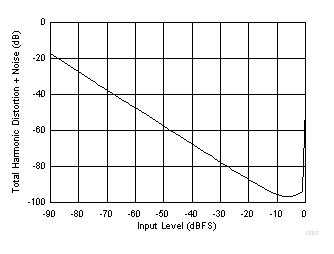
PCM1860 PCM1861 PCM1862 PCM1863 PCM1864 PCM1865 D001_SLASE64.gif
PCM1861, PCM1863, and PCM1865
Figure 6. THD+N vs Input Level
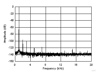
PCM1860 PCM1861 PCM1862 PCM1863 PCM1864 PCM1865 D003_SLASE64.gif
PCM1861, PCM1863, and PCM1865
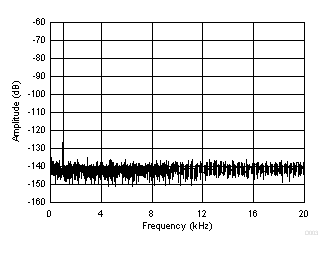
Input = –60 dBFS at 1 kHz
Figure 8. Main ADC Output FFT
PCM1860 PCM1861 PCM1862 PCM1863 PCM1864 PCM1865 D005_SLASE64.gif
PCM1861, PCM1863, and PCM1865
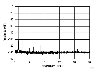
Input = –1 dBFS at 1 kHz
Figure 10. Main ADC Output FFT
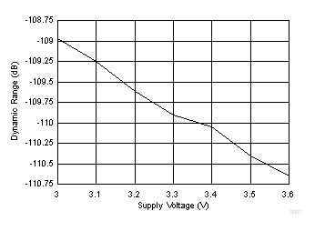
PCM1860 PCM1861 PCM1862 PCM1863 PCM1864 PCM1865 D007_SLASE64.gif
PCM1861, PCM1863, and PCM1865
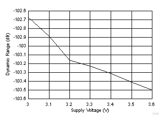
Figure 12. Dynamic Range vs Supply Voltage
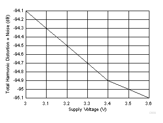
PCM1860 PCM1861 PCM1862 PCM1863 PCM1864 PCM1865 D009_SLASE64.gif
PCM1861, PCM1863, and PCM1865
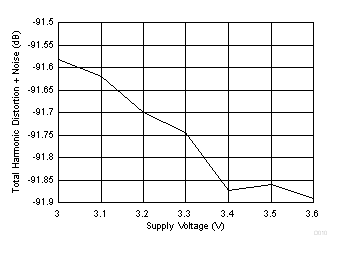
Figure 14. THD+N vs Supply Voltage
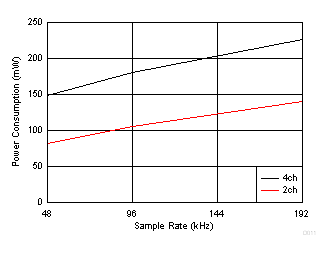
PCM1860 PCM1861 PCM1862 PCM1863 PCM1864 PCM1865 D011_SLASE64.gif
At fS = 48 kHz, 96 kHz, and 192 kHz
Figure 16. Power Consumption vs Sample Rate
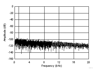
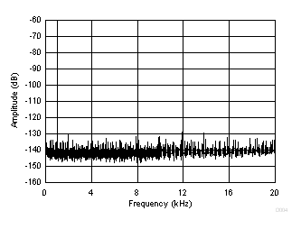
PCM1860 PCM1861 PCM1862 PCM1863 PCM1864 PCM1865 D013_SLASE64.gif
fS = 48 kHz
Figure 18. Secondary ADC FFT
PCM1860 PCM1861 PCM1862 PCM1863 PCM1864 PCM1865 D015_SLASE64.gif
Figure 20. PGA ADC Gain
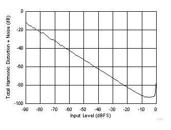
PCM1860 PCM1861 PCM1862 PCM1863 PCM1864 PCM1865 D002_SLASE64.gif
PCM1860, PCM1862, and PCM1864
Figure 7. THD+N vs Input Level
PCM1860 PCM1861 PCM1862 PCM1863 PCM1864 PCM1865 D004_SLASE64.gif
PCM1860, PCM1862, and PCM1864
Input = –60 dBFS at 1 kHz
Figure 9. Main ADC Output FFT
PCM1860 PCM1861 PCM1862 PCM1863 PCM1864 PCM1865 D006_SLASE64.gif
PCM1860, PCM1862, and PCM1864
Input = –1 dBFS at 1 kHz
Figure 11. Main ADC Output FFT
PCM1860 PCM1861 PCM1862 PCM1863 PCM1864 PCM1865 D008_SLASE64.gif
PCM1860, PCM1862, and PCM1864
Figure 13. Dynamic Range vs Supply Voltage
PCM1860 PCM1861 PCM1862 PCM1863 PCM1864 PCM1865 D010_SLASE64.gif
PCM1860, PCM1862, and PCM1864
Figure 15. THD+N vs Supply Voltage
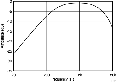
PCM1860 PCM1861 PCM1862 PCM1863 PCM1864 PCM1865 D012_SLASE64.gif
fS = 48 kHz
Figure 17. Secondary ADC Frequency Response
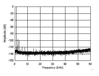
PCM1860 PCM1861 PCM1862 PCM1863 PCM1864 PCM1865 D014_SLASE64.gif
fS = 192 kHz, BW = 60 kHz, Input = –1 dBFS
Figure 19. High Bandwidth FFT of THD Components
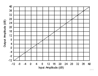
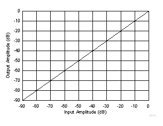
PCM1860 PCM1861 PCM1862 PCM1863 PCM1864 PCM1865 D016_SLASE64.gif
Figure 21. Linearity, Input vs Output