SLAS724A September 2008 – November 2014 PCM3070
PRODUCTION DATA.
- 1 Features
- 2 Applications
- 3 Description
- 4 Simplified Schematic
- 5 Revision History
- 6 Device Comparison Table
- 7 Pin Configuration and Functions
-
8 Specifications
- 8.1 Absolute Maximum Ratings
- 8.2 Handling Ratings
- 8.3 Recommended Operating Conditions
- 8.4 Thermal Information
- 8.5 Electrical Characteristics, ADC
- 8.6 Electrical Characteristics, Bypass Outputs
- 8.7 Electrical Characteristics, Audio DAC Outputs
- 8.8 Electrical Characteristics, LDO
- 8.9 Electrical Characteristics, Misc.
- 8.10 Electrical Characteristics, Logic Levels
- 8.11 I2S LJF and RJF Timing in Master Mode (see )
- 8.12 I2S LJF and RJF Timing in Slave Mode (see )
- 8.13 DSP Timing in Master Mode (see )
- 8.14 DSP Timing in Slave Mode (see )
- 8.15 I2C Interface Timing
- 8.16 SPI Interface Timing (See )
- 8.17 Typical Characteristics
- 9 Parameter Measurement Information
- 10Detailed Description
- 11Application and Implementation
- 12Power Supply Recommendations
- 13Layout
- 14Device and Documentation Support
- 15Mechanical, Packaging, and Orderable Information
Package Options
Mechanical Data (Package|Pins)
- RHB|32
Thermal pad, mechanical data (Package|Pins)
- RHB|32
Orderable Information
10 Detailed Description
10.1 Overview
The PCM3070 features two fully-programmable miniDSP cores that support application-specific algorithms in the record and/or the playback path of the device. The miniDSP cores are fully software controlled. Target algorithms, like speaker EQ, Crossovers, Dynamic Range Controls, Intelligent volume controls and other post-processing algorithms are loaded into the device after power-up.
Extensive register-based control of input/output channel configuration, gains, effects, pin-multiplexing and clocks is included, allowing the device to be precisely targeted to its application.
The record path of the PCM3070 covers operations from 8kHz mono to 192kHz stereo recording, and contains programmable input channel configurations covering single-ended and differential setups, as well as floating or mixed input signals.
The playback path offers signal-processing blocks for filtering and effects, and supports flexible mixing of DAC and analog input signals as well as programmable volume controls. The playback path contains two high-power output drivers as well as two fully-differential outputs. The high-power outputs can be configured in multiple ways, including stereo and mono BTL.
The voltage supply range for the PCM3070 for analog is 1.5V–1.95V, and for digital it is 1.26V–1.95V. To ease system-level design, LDOs are integrated to generate the appropriate analog or digital supply from input voltages ranging from 1.8V to 3.6V. Digital I/O voltages are supported in the range of 1.5V–3.6V.
The required internal clock of the PCM3070 can be derived from multiple sources, including the MCLK pin, the BCLK pin, the GPIO pin or the output of the internal PLL, where the input to the PLL again can be derived from the MCLK pin, the BCLK or GPIO pins. The PLL is highly programmable and can accept available input clocks in the range of 512kHz to 50MHz.
10.2 Functional Block Diagram
Figure 18 shows the basic functional blocks of the device.
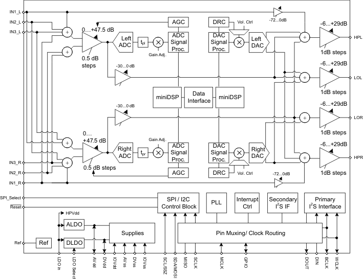 Figure 18. Block Diagram
10.3 Feature Description
10.3.1 Device Connections
10.3.1.1 Digital Pins
Only a small number of digital pins are dedicated to a single function; whenever possible, the digital pins have a default function, and also can be reprogrammed to cover alternative functions for various applications.
The fixed-function pins are Reset and the SPI_Select pin, which are HW control pins. Depending on the state of SPI_Select, the two control-bus pins SCL/SS and SDA/MOSI are configured for either I2C or SPI protocol.
Other digital IO pins can be configured for various functions via register control. An overview of available functionality is given in Multifunction Pins.
10.3.1.1.1 Multifunction Pins
Table 1 shows the possible allocation of pins for specific functions. The PLL input, for example, can be programmed to be any of 4 pins (MCLK, BCLK, DIN, GPIO).
Table 1. Multifunction Pin Assignments
| 1 | 2 | 3 | 4 | 5 | 6 | 7 | 8 | ||
|---|---|---|---|---|---|---|---|---|---|
| Pin Function | MCLK | BCLK | WCLK | DIN MFP1 |
DOUT MFP2 |
MFP3/ SCLK |
MFP4/ MISO |
GPIO MFP5 |
|
| A | PLL Input | S(2) | S(3) | E | S(4) | ||||
| B | Codec Clock Input | S(2),D(5) | S(3) | S(4) | |||||
| C | I2S BCLK input | S,D | |||||||
| D | I2S BCLK output | E(1) | |||||||
| E | I2S WCLK input | E, D | |||||||
| F | I2S WCLK output | E | |||||||
| G | I2S ADC word clock input | E | E | ||||||
| H | I2S ADC WCLK out | E | E | ||||||
| I | I2S DIN | E, D | |||||||
| J | I2S DOUT | E, D | |||||||
| K | General Purpose Output I | E | |||||||
| K | General Purpose Output II | E | |||||||
| K | General Purpose Output III | E | |||||||
| L | General Purpose Input I | E | |||||||
| L | General Purpose Input II | E | |||||||
| L | General Purpose Input III | E | |||||||
| M | INT1 output | E | E | E | |||||
| N | INT2 output | E | E | E | |||||
| Q | Secondary I2S BCLK input | E | E | ||||||
| R | Secondary I2S WCLK in | E | E | ||||||
| S | Secondary I2S DIN | E | E | ||||||
| T | Secondary I2S DOUT | E | |||||||
| U | Secondary I2S BCLK OUT | E | E | E | |||||
| V | Secondary I2S WCLK OUT | E | E | E | |||||
| W | Reserved | ||||||||
| X | Aux Clock Output | E | E | E |
10.3.1.2 Analog Pins
Analog functions can also be configured to a large degree. Analog blocks are powered down by default. The blocks can be powered up with fine granularity according to the application needs.
10.3.2 Analog Audio I/O
The analog IO path of the PCM3070 features a large set of options for signal conditioning as well as signal routing:
- 6 analog inputs which can be mixed and-or multiplexed in single-ended and-or differential configuration
- 2 programmable gain amplifiers (PGA) with a range of 0 to +47.5dB
- 2 mixer amplifiers for analog bypass
- 2 low power analog bypass channels
- Mute function
- Automatic gain control (AGC)
- Channel-to-channel phase adjustment
- Fast charge of ac-coupling capacitors
- Anti thump
10.3.2.1 Analog Bypass
The PCM3070 offers two analog-bypass modes. In either of the modes, an analog input signal can be routed from an analog input pin to an amplifier driving an analog output pin. Neither the ADC nor the DAC resources are required for such operation.
In analog low-power bypass mode, line-level signals can be routed directly from the analog inputs INL to the left headphone amplifier (HPL) and INR to HPR.
10.3.2.2 ADC Bypass Using Mixer Amplifiers
In addition to the analog bypass mode, another bypass mode uses the programmable gain amplifiers of the input stage in conjunction with a mixer amplifier. With this mode, low-level signals can be amplified and routed to the line or headphone outputs, fully bypassing the ADC and DAC.
To enable this mode, the mixer amplifiers are powered on via software command.
10.3.2.3 Headphone Output
The stereo headphone drivers on pins HPL and HPR can drive loads with impedances down to 16Ω in single-ended AC-coupled headphone configurations, or loads down to 32Ω in differential mode, where a speaker is connected between HPL and HPR. In single-ended drive configuration these drivers can drive up to 15mW power into each headphone channel while operating from 1.8V analog supplies. While running from the AVdd supply, the output common-mode of the headphone driver is set by the common-mode setting of analog inputs in Page 1 / Register 10, Bit D6, to allow maximum utilization of the analog supply range while simultaneously providing a higher output-voltage swing. In cases when higher output-voltage swing is required, the headphone amplifiers can run directly from the higher supply voltage on LDOIN input (up to 3.6V). To use the higher supply voltage for higher output signal swing, the output common-mode can be adjusted to either 1.25V, 1.5V or 1.65V by configuring Page 1 / Register 10, Bits D5-D4. When the common-mode voltage is configured at 1.65V and LDOIN supply is 3.3V, the headphones can each deliver up to 40mW power into a 16Ω load.
The headphone drivers are capable of driving a mixed combination of DAC signal and bypass from analog input INL and INR by configuring Page 1 / Register 12 and Page 1 / Register 13 respectively. The analog input signals can be attenuated up to 72dB before routing by configuring Page 1 / Register 22 and 23. The level of the DAC signal can be controlled using the digital volume control of the DAC in Page 0, Reg 65 and 66. To control the output-voltage swing of headphone drivers, the digital volume control provides a range of –6.0dB to +29.0dB(6) in steps of 1dB. These can be configured by programming Page 1 / Register 16 and 17. These level controls are not meant to be used as dynamic volume control, but more to set output levels during initial device configuration.
10.3.2.4 Line Outputs
The stereo line level drivers on LOL and LOR pins can drive a wide range of line level resistive impedances in the range of 600Ω to 10kΩ. The output common modes of line level drivers can be configured to equal either the analog input common-mode setting, or 1.65V. With output common-mode setting of 1.65V and DRVdd_HP supply at 3.3V the line-level drivers can drive up to 1Vrms output signal. The line-level drivers can drive out a mixed combination of DAC signal and attenuated ADC PGA signal. Signal mixing is register-programmable.
10.3.3 ADC
The PCM3070 includes a stereo audio ADC, which uses a delta-sigma modulator with a programmable oversampling ratio, followed by a digital decimation filter. The stereo recording path can be powered up one channel at a time, to support the case where only mono record capability is required.
The ADC path of the PCM3070 features a large set of options for signal conditioning as well as signal routing:
- Two ADCs
- Six analog inputs which can be mixed and-or multiplexed in single-ended and-or differential configuration
- Two programmable gain amplifiers (PGA) with a range of 0 to +47.5dB
- Two mixer amplifiers for analog bypass
- Two analog bypass channels
- Fine gain adjustment of digital channels with 0.1dB step size
- Digital volume control with a range of -12 to +20dB
- Mute function
- Automatic gain control (AGC)
In addition to the standard set of ADC features the PCM3070 also offers the following special functions:
- Channel-to-channel phase adjustment
- Fast charge of ac-coupling capacitors
- Anti thump
- Adaptive filter mode
10.3.3.1 ADC Processing
The PCM3070 offers a range of processing blocks which implement various signal processing capabilities along with decimation filtering. These processing blocks give users the choice of how much and what type of signal processing they may use and which decimation filter is applied.
10.3.3.1.1 ADC Processing Blocks
The PCM3070 offers a range of processing blocks which implement various signal processing capabilities along with decimation filtering. These processing blocks give users the choice of how much and what type of signal processing they may use and which decimation filter is applied.
Table 2 gives an overview of the available processing blocks and their properties.
The signal processing blocks available are:
- First-order IIR
- Scalable number of biquad filters
- Variable-tap FIR filter
- AGC
The processing blocks are tuned for common cases and can achieve high anti-alias filtering or low group delay in combination with various signal processing effects such as audio effects and frequency shaping. The available first order IIR, BiQuad and FIR filters have fully user-programmable coefficients. The Resource Class Column (RC) gives an approximate indication of power consumption.
Table 2. ADC Processing Blocks
| Processing Blocks | Channel | Decimation Filter |
1st Order IIR Available |
Number BiQuads |
FIR | Required AOSR Value | Resource Class |
|---|---|---|---|---|---|---|---|
| PRB_R1(1) | Stereo | A | Yes | 0 | No | 128,64 | 6 |
| PRB_R2 | Stereo | A | Yes | 5 | No | 128,64 | 8 |
| PRB_R3 | Stereo | A | Yes | 0 | 25-Tap | 128,64 | 8 |
| PRB_R4 | Right | A | Yes | 0 | No | 128,64 | 3 |
| PRB_R5 | Right | A | Yes | 5 | No | 128,64 | 4 |
| PRB_R6 | Right | A | Yes | 0 | 25-Tap | 128,64 | 4 |
| PRB_R7 | Stereo | B | Yes | 0 | No | 64 | 3 |
| PRB_R8 | Stereo | B | Yes | 3 | No | 64 | 4 |
| PRB_R9 | Stereo | B | Yes | 0 | 20-Tap | 64 | 4 |
| PRB_R10 | Right | B | Yes | 0 | No | 64 | 2 |
| PRB_R11 | Right | B | Yes | 3 | No | 64 | 2 |
| PRB_R12 | Right | B | Yes | 0 | 20-Tap | 64 | 2 |
| PRB_R13 | Stereo | C | Yes | 0 | No | 32 | 3 |
| PRB_R14 | Stereo | C | Yes | 5 | No | 32 | 4 |
| PRB_R15 | Stereo | C | Yes | 0 | 25-Tap | 32 | 4 |
| PRB_R16 | Right | C | Yes | 0 | No | 32 | 2 |
| PRB_R17 | Right | C | Yes | 5 | No | 32 | 2 |
| PRB_R18 | Right | C | Yes | 0 | 25-Tap | 32 | 2 |
For more detailed information see the PCM3070 Application Reference Guide, SLAU332.
10.3.4 DAC
The PCM3070 includes a stereo audio DAC supporting data rates from 8kHz to 192kHz. Each channel of the stereo audio DAC consists of a signal-processing engine with fixed processing blocks, a programmable miniDSP, a digital interpolation filter, multi-bit digital delta-sigma modulator, and an analog reconstruction filter. The DAC is designed to provide enhanced performance at low sampling rates through increased oversampling and image filtering, thereby keeping quantization noise generated within the delta-sigma modulator and signal images strongly suppressed within the audio band to beyond 20kHz. To handle multiple input rates and optimize performance, the PCM3070 allows the system designer to program the oversampling rates over a wide range from 1 to 1024. The system designer can choose higher oversampling ratios for lower input data rates and lower oversampling ratios for higher input data rates.
The PCM3070 DAC channel includes a built-in digital interpolation filter to generate oversampled data for the sigma-delta modulator. The interpolation filter can be chosen from three different types depending on required frequency response, group delay and sampling rate.
The DAC path of the PCM3070 features many options for signal conditioning and signal routing:
- 2 headphone amplifiers
- Usable in single-ended or differential mode
- Analog volume setting with a range of -6 to +29dB
- 2 line-out amplifiers
- Usable in single-ended or differential mode
- Analog volume setting with a range of -6 to +29dB
- Digital volume control with a range of -63.5 to +24dB
- Mute function
- Dynamic range compression (DRC)
In addition to the standard set of DAC features the PCM3070 also offers the following special features:
- Built in sine wave generation (beep generator)
- Digital auto mute
- Adaptive filter mode
10.3.4.1 DAC Processing Blocks — Overview
The PCM3070 implements signal processing capabilities and interpolation filtering via processing blocks. These fixed processing blocks give users the choice of how much and what type of signal processing they may use and which interpolation filter is applied.
Table 3 gives an overview over all available processing blocks of the DAC channel and their properties. The Resource Class Column (RC) gives an approximate indication of power consumption.
The signal processing blocks available are:
- First-order IIR
- Scalable number of biquad filters
- 3D – Effect
- Beep Generator
The processing blocks are tuned for typical cases and can achieve high image rejection or low group delay in combination with various signal processing effects such as audio effects and frequency shaping. The available first-order IIR and biquad filters have fully user-programmable coefficients. The Resource Class Column (RC) gives an approximate indication of power consumption.
Table 3. Overview – DAC Predefined Processing Blocks
| Processing Block No. |
Interpolation Filter | Channel | 1st Order IIR Available |
Num. of Biquads | DRC | 3D | Beep Generator |
|---|---|---|---|---|---|---|---|
| PRB_P1(1) | A | Stereo | No | 3 | No | No | No |
| PRB_P2 | A | Stereo | Yes | 6 | Yes | No | No |
| PRB_P3 | A | Stereo | Yes | 6 | No | No | No |
| PRB_P4 | A | Left | No | 3 | No | No | No |
| PRB_P5 | A | Left | Yes | 6 | Yes | No | No |
| PRB_P6 | A | Left | Yes | 6 | No | No | No |
| PRB_P7 | B | Stereo | Yes | 0 | No | No | No |
| PRB_P8 | B | Stereo | No | 4 | Yes | No | No |
| PRB_P9 | B | Stereo | No | 4 | No | No | No |
| PRB_P10 | B | Stereo | Yes | 6 | Yes | No | No |
| PRB_P11 | B | Stereo | Yes | 6 | No | No | No |
| PRB_P12 | B | Left | Yes | 0 | No | No | No |
| PRB_P13 | B | Left | No | 4 | Yes | No | No |
| PRB_P14 | B | Left | No | 4 | No | No | No |
| PRB_P15 | B | Left | Yes | 6 | Yes | No | No |
| PRB_P16 | B | Left | Yes | 6 | No | No | No |
| PRB_P17 | C | Stereo | Yes | 0 | No | No | No |
| PRB_P18 | C | Stereo | Yes | 4 | Yes | No | No |
| PRB_P19 | C | Stereo | Yes | 4 | No | No | No |
| PRB_P20 | C | Left | Yes | 0 | No | No | No |
| PRB_P21 | C | Left | Yes | 4 | Yes | No | No |
| PRB_P22 | C | Left | Yes | 4 | No | No | No |
| PRB_P23 | A | Stereo | No | 2 | No | Yes | No |
| PRB_P24 | A | Stereo | Yes | 5 | Yes | Yes | No |
| PRB_P25 | A | Stereo | Yes | 5 | Yes | Yes | Yes |
For more detailed information see the PCM3070 Application Reference Guide, SLAU332.
10.3.5 Digital Audio IO Interface
Audio data is transferred between the host processor and the PCM3070 via the digital audio data serial interface, or audio bus. The audio bus on this device is very flexible, including left or right-justified data options, support for I2S or PCM protocols, programmable data length options, a TDM mode for multichannel operation, very flexible master/slave configurability for each bus clock line, and the ability to communicate with multiple devices within a system directly.
The audio bus of the PCM3070 can be configured for left or right-justified, I2S, DSP, or TDM modes of operation, where communication with standard PCM interfaces is supported within the TDM mode. These modes are all MSB-first, with data width programmable as 16, 20, 24, or 32 bits by configuring Page 0, Register 27, D(5:4). In addition, the word clock and bit clock can be independently configured in either Master or Slave mode, for flexible connectivity to a wide variety of processors. The word clock is used to define the beginning of a frame, and may be programmed as either a pulse or a square-wave signal. The frequency of this clock corresponds to the maximum of the selected ADC and DAC sampling frequencies.
The bit clock is used to clock in and clock out the digital audio data across the serial bus. When in Master mode, this signal can be programmed to generate variable clock pulses by controlling the bit-clock divider in Page 0, Register 30. The number of bit-clock pulses in a frame may need adjustment to accommodate various word-lengths as well as to support the case when multiple PCM3070s may share the same audio bus.
The PCM3070 also includes a feature to offset the position of start of data transfer with respect to the word-clock. This offset can be controlled in terms of number of bit-clocks and can be programmed in Page 0, Register 28.
The PCM3070 also has the feature of inverting the polarity of the bit-clock used for transferring the audio data as compared to the default clock polarity used. This feature can be used independently of the mode of audio interface chosen. This can be configured via Page 0, Register 29, D(3).
The PCM3070 further includes programmability (Page 0, Register 27, D0) to place the DOUT line into a hi-Z (3-state) condition during all bit clocks when valid data is not being sent. By combining this capability with the ability to program at what bit clock in a frame the audio data begins, time-division multiplexing (TDM) can be accomplished, enabling the use of multiple codecs on a single audio serial data bus. When the audio serial data bus is powered down while configured in master mode, the pins associated with the interface are put into a hi-Z output condition.
By default when the word-clocks and bit-clocks are generated by the PCM3070, these clocks are active only when the codec (ADC, DAC or both) are powered up within the device. This is done to save power. However, it also supports a feature when both the word clocks and bit-clocks can be active even when the codec in the device is powered down. This is useful when using the TDM mode with multiple codecs on the same bus, or when word-clock or bit-clocks are used in the system as general-purpose clocks.
10.3.6 Clock Generation and PLL
The PCM3070 supports a wide range of options for generating clocks for the ADC and DAC sections as well as interface and other control blocks. The clocks for ADC and DAC require a source reference clock. This clock can be provided on variety of device pins such as MCLK, BCLK or GPI pins. The CODEC_CLKIN can then be routed through highly-flexible clock dividers to generate the various clocks required for ADC, DAC and the miniDSP sections. In the event that the desired audio or miniDSP clocks cannot be generated from the reference clocks on MCLK BCLK or GPIO, the PCM3070 also provides the option of using the on-chip PLL which supports a wide range of fractional multiplication values to generate the required clocks. Starting from CODEC_CLKIN the PCM3070 provides several programmable clock dividers to help achieve a variety of sampling rates for ADC, DAC and clocks for the miniDSP.
For more detailed information see the PCM3070 Application Reference Guide, SLAU332.
10.3.7 Control Interfaces
The PCM3070 control interface supports SPI or I2C communication protocols, with the protocol selectable using the SPI_SELECT pin. For SPI, SPI_SELECT should be tied high; for I2C, SPI_SELECT should be tied low. Changing the state of SPI_SELECT during device operation is not recommended.
10.3.7.1 I2C Control
The PCM3070 supports the I2C control protocol, and will respond to the I2C address of 0011000. I2C is a two-wire, open-drain interface supporting multiple devices and masters on a single bus. Devices on the I2C bus only drive the bus lines LOW by connecting them to ground; they never drive the bus lines HIGH. Instead, the bus wires are pulled HIGH by pullup resistors, so the bus wires are HIGH when no device is driving them LOW. This circuit prevents two devices from conflicting; if two devices drive the bus simultaneously, there is no driver contention.
10.3.7.2 SPI Control
In the SPI control mode, the PCM3070 uses the pins SCL/SS as SS, SCLK as SCLK, MISO as MISO, SDA/MOSI as MOSI; a standard SPI port with clock polarity setting of 0 (typical microprocessor SPI control bit CPOL = 0). The SPI port allows full-duplex, synchronous, serial communication between a host processor (the master) and peripheral devices (slaves). The SPI master (in this case, the host processor) generates the synchronizing clock (driven onto SCLK) and initiates transmissions. The SPI slave devices (such as the PCM3070) depend on a master to start and synchronize transmissions. A transmission begins when initiated by an SPI master. The byte from the SPI master begins shifting in on the slave MOSI pin under the control of the master serial clock (driven onto SCLK). As the byte shifts in on the MOSI pin, a byte shifts out on the MISO pin to the master shift register.
For more detailed information see the PCM3070 Application Reference Guide, SLAU332.
10.4 Device Functional Modes
The following special functions are available to support advanced system requirements:
- Interrupt generation
- Flexible pin multiplexing
For more detailed information see the PCM3070 Application Reference Guide, SLAU332.
10.4.1 MiniDSP
The PCM3070 features two miniDSP cores. The first miniDSP core is tightly coupled to the ADC, the second miniDSP core is tightly coupled to the DAC. The fully programmable algorithms for the miniDSP must be loaded into the device after power up. The miniDSPs have direct access to the digital stereo audio stream on the ADC and on the DAC side, offering the possibility for advanced, very-low group delay DSP algorithms. Each miniDSP can run up to 1152 instructions on every audio sample at a 48kHz sample rate. The two cores can run fully synchronized and can exchange data.
10.4.2 Software
Software development for the PCM3070 is supported through TI's comprehensive PurePath Studio Development Environment; a powerful, easy-to-use tool designed specifically to simplify software development on the PCM3070 miniDSP audio platform. The Graphical Development Environment consists of a library of common audio functions that can be dragged-and-dropped into an audio signal flow and graphically connected together. The DSP code can then be assembled from the graphical signal flow with the click of a mouse.
Please visit the PCM3070 product folder on www.ti.com to learn more about PurePath Studio and the latest status on available, ready-to-use DSP algorithms.
10.5 Register Map
10.5.1 Register Map Summary
Table 4. Summary of Register Map
| Decimal | Hex | DESCRIPTION | ||
|---|---|---|---|---|
| PAGE NO. | REG. NO. | PAGE NO. | REG. NO. | |
| 0 | 0 | 0x00 | 0x00 | Page Select Register |
| 0 | 1 | 0x00 | 0x01 | Software Reset Register |
| 0 | 2 | 0x00 | 0x02 | Reserved Register |
| 0 | 3 | 0x00 | 0x03 | Reserved Register |
| 0 | 4 | 0x00 | 0x04 | Clock Setting Register 1, Multiplexers |
| 0 | 5 | 0x00 | 0x05 | Clock Setting Register 2, PLL P&R Values |
| 0 | 6 | 0x00 | 0x06 | Clock Setting Register 3, PLL J Values |
| 0 | 7 | 0x00 | 0x07 | Clock Setting Register 4, PLL D Values (MSB) |
| 0 | 8 | 0x00 | 0x08 | Clock Setting Register 5, PLL D Values (LSB) |
| 0 | 9-10 | 0x00 | 0x09-0x0A | Reserved Register |
| 0 | 11 | 0x00 | 0x0B | Clock Setting Register 6, NDAC Values |
| 0 | 12 | 0x00 | 0x0C | Clock Setting Register 7, MDAC Values |
| 0 | 13 | 0x00 | 0x0D | DAC OSR Setting Register 1, MSB Value |
| 0 | 14 | 0x00 | 0x0E | DAC OSR Setting Register 2, LSB Value |
| 0 | 15 | 0x00 | 0x0F | miniDSP_D Instruction Control Register 1 |
| 0 | 16 | 0x00 | 0x10 | miniDSP_D Instruction Control Register 2 |
| 0 | 17 | 0x00 | 0x11 | miniDSP_D Interpolation Factor Setting Register |
| 0 | 18 | 0x00 | 0x12 | Clock Setting Register 8, NADC Values |
| 0 | 19 | 0x00 | 0x13 | Clock Setting Register 9, MADC Values |
| 0 | 20 | 0x00 | 0x14 | ADC Oversampling (AOSR) Register |
| 0 | 21 | 0x00 | 0x15 | miniDSP_A Instruction Control Register 1 |
| 0 | 22 | 0x00 | 0x16 | miniDSP_A Instruction Control Register 2 |
| 0 | 23 | 0x00 | 0x17 | miniDSP_A Decimation Factor Setting Register |
| 0 | 24 | 0x00 | 0x18 | Reserved Register |
| 0 | 25 | 0x00 | 0x19 | Clock Setting Register 10, Multiplexers |
| 0 | 26 | 0x00 | 0x1A | Clock Setting Register 11, CLKOUT M divider value |
| 0 | 27 | 0x00 | 0x1B | Audio Interface Setting Register 1 |
| 0 | 28 | 0x00 | 0x1C | Audio Interface Setting Register 2, Data offset setting |
| 0 | 29 | 0x00 | 0x1D | Audio Interface Setting Register 3 |
| 0 | 30 | 0x00 | 0x1E | Clock Setting Register 12, BCLK N Divider |
| 0 | 31 | 0x00 | 0x1F | Audio Interface Setting Register 4, Secondary Audio Interface |
| 0 | 32 | 0x00 | 0x20 | Audio Interface Setting Register 5 |
| 0 | 33 | 0x00 | 0x21 | Audio Interface Setting Register 6 |
| 0 | 34 | 0x00 | 0x22 | Digital Interface Misc. Setting Register |
| 0 | 35 | 0x00 | 0x23 | Reserved Register |
| 0 | 36 | 0x00 | 0x24 | ADC Flag Register |
| 0 | 37 | 0x00 | 0x25 | DAC Flag Register 1 |
| 0 | 38 | 0x00 | 0x26 | DAC Flag Register 2 |
| 0 | 39-41 | 0x00 | 0x27-0x29 | Reserved Register |
| 0 | 42 | 0x00 | 0x2A | Sticky Flag Register 1 |
| 0 | 43 | 0x00 | 0x2B | Interrupt Flag Register 1 |
| 0 | 44 | 0x00 | 0x2C | Sticky Flag Register 2 |
| 0 | 45 | 0x00 | 0x2D | Sticky Flag Register 3 |
| 0 | 46 | 0x00 | 0x2E | Interrupt Flag Register 2 |
| 0 | 47 | 0x00 | 0x2F | Interrupt Flag Register 3 |
| 0 | 48 | 0x00 | 0x30 | INT1 Interrupt Control Register |
| 0 | 49 | 0x00 | 0x31 | INT2 Interrupt Control Register |
| 0 | 50-51 | 0x00 | 0x32-0x33 | Reserved Register |
| 0 | 52 | 0x00 | 0x34 | GPIO/MFP5 Control Register |
| 0 | 53 | 0x00 | 0x35 | DOUT/MFP2 Function Control Register |
| 0 | 54 | 0x00 | 0x36 | DIN/MFP1 Function Control Register |
| 0 | 55 | 0x00 | 0x37 | MISO/MFP4 Function Control Register |
| 0 | 56 | 0x00 | 0x38 | SCLK/MFP3 Function Control Register |
| 0 | 57-59 | 0x00 | 0x39-0x3B | Reserved Registers |
| 0 | 60 | 0x00 | 0x3C | DAC Signal Processing Block Control Register |
| 0 | 61 | 0x00 | 0x3D | ADC Signal Processing Block Control Register |
| 0 | 62 | 0x00 | 0x3E | miniDSP_A and miniDSP_D Configuration Register |
| 0 | 63 | 0x00 | 0x3F | DAC Channel Setup Register 1 |
| 0 | 64 | 0x00 | 0x40 | DAC Channel Setup Register 2 |
| 0 | 65 | 0x00 | 0x41 | Left DAC Channel Digital Volume Control Register |
| 0 | 66 | 0x00 | 0x42 | Right DAC Channel Digital Volume Control Register |
| 0 | 67 | 0x00 | 0x43 | Headset Detection Configuration Register |
| 0 | 68 | 0x00 | 0x44 | DRC Control Register 1 |
| 0 | 69 | 0x00 | 0x45 | DRC Control Register 2 |
| 0 | 70 | 0x00 | 0x46 | DRC Control Register 3 |
| 0 | 71 | 0x00 | 0x47 | Beep Generator Register 1 |
| 0 | 72 | 0x00 | 0x48 | Beep Generator Register 2 |
| 0 | 73 | 0x00 | 0x49 | Beep Generator Register 3 |
| 0 | 74 | 0x00 | 0x4A | Beep Generator Register 4 |
| 0 | 75 | 0x00 | 0x4B | Beep Generator Register 5 |
| 0 | 76 | 0x00 | 0x4C | Beep Generator Register 6 |
| 0 | 77 | 0x00 | 0x4D | Beep Generator Register 7 |
| 0 | 78 | 0x00 | 0x4E | Beep Generator Register 8 |
| 0 | 79 | 0x00 | 0x4F | Beep Generator Register 9 |
| 0 | 80 | 0x00 | 0x50 | Reserved Register |
| 0 | 81 | 0x00 | 0x51 | ADC Channel Setup Register |
| 0 | 82 | 0x00 | 0x52 | ADC Fine Gain Adjust Register |
| 0 | 83 | 0x00 | 0x53 | Left ADC Channel Volume Control Register |
| 0 | 84 | 0x00 | 0x54 | Right ADC Channel Volume Control Register |
| 0 | 85 | 0x00 | 0x55 | ADC Phase Adjust Register |
| 0 | 86 | 0x00 | 0x56 | Left Channel AGC Control Register 1 |
| 0 | 87 | 0x00 | 0x57 | Left Channel AGC Control Register 2 |
| 0 | 88 | 0x00 | 0x58 | Left Channel AGC Control Register 3 |
| 0 | 89 | 0x00 | 0x59 | Left Channel AGC Control Register 4 |
| 0 | 90 | 0x00 | 0x5A | Left Channel AGC Control Register 5 |
| 0 | 91 | 0x00 | 0x5B | Left Channel AGC Control Register 6 |
| 0 | 92 | 0x00 | 0x5C | Left Channel AGC Control Register 7 |
| 0 | 93 | 0x00 | 0x5D | Left Channel AGC Control Register 8 |
| 0 | 94 | 0x00 | 0x5E | Right Channel AGC Control Register 1 |
| 0 | 95 | 0x00 | 0x5F | Right Channel AGC Control Register 2 |
| 0 | 96 | 0x00 | 0x60 | Right Channel AGC Control Register 3 |
| 0 | 97 | 0x00 | 0x61 | Right Channel AGC Control Register 4 |
| 0 | 98 | 0x00 | 0x62 | Right Channel AGC Control Register 5 |
| 0 | 99 | 0x00 | 0x63 | Right Channel AGC Control Register 6 |
| 0 | 100 | 0x00 | 0x64 | Right Channel AGC Control Register 7 |
| 0 | 101 | 0x00 | 0x65 | Right Channel AGC Control Register 8 |
| 0 | 102 | 0x00 | 0x66 | DC Measurement Register 1 |
| 0 | 103 | 0x00 | 0x67 | DC Measurement Register 2 |
| 0 | 104 | 0x00 | 0x68 | Left Channel DC Measurement Output Register 1 |
| 0 | 105 | 0x00 | 0x69 | Left Channel DC Measurement Output Register 2 |
| 0 | 106 | 0x00 | 0x6A | Left Channel DC Measurement Output Register 3 |
| 0 | 107 | 0x00 | 0x6B | Right Channel DC Measurement Output Register 1 |
| 0 | 108 | 0x00 | 0x6C | Right Channel DC Measurement Output Register 2 |
| 0 | 109 | 0x00 | 0x6D | Right Channel DC Measurement Output Register 3 |
| 0 | 110-127 | 0x00 | 0x6E-0x7F | Reserved Register |
| 1 | 0 | 0x01 | 0x00 | Page Select Register |
| 1 | 1 | 0x01 | 0x01 | LDO Control Register |
| 1 | 2 | 0x01 | 0x02 | Power Configuration Register 2 |
| 1 | 3 | 0x01 | 0x03 | Playback Configuration Register 1 |
| 1 | 4 | 0x01 | 0x04 | Playback Configuration Register 2 |
| 1 | 5-8 | 0x01 | 0x05-0x08 | Reserved Register |
| 1 | 9 | 0x01 | 0x09 | Output Driver Power Control Register |
| 1 | 10 | 0x01 | 0x0A | Common Mode Control Register |
| 1 | 11 | 0x01 | 0x0B | Over Current Protection Configuration Register |
| 1 | 12 | 0x01 | 0x0C | HPL Routing Selection Register |
| 1 | 13 | 0x01 | 0x0D | HPR Routing Selection Register |
| 1 | 14 | 0x01 | 0x0E | LOL Routing Selection Register |
| 1 | 15 | 0x01 | 0x0F | LOR Routing Selection Register |
| 1 | 16 | 0x01 | 0x10 | HPL Driver Gain Setting Register |
| 1 | 17 | 0x01 | 0x11 | HPR Driver Gain Setting Register |
| 1 | 18 | 0x01 | 0x12 | LOL Driver Gain Setting Register |
| 1 | 19 | 0x01 | 0x13 | LOR Driver Gain Setting Register |
| 1 | 20 | 0x01 | 0x14 | Headphone Driver Startup Control Register |
| 1 | 21 | 0x01 | 0x15 | Reserved Register |
| 1 | 22 | 0x01 | 0x16 | IN1L to HPL Volume Control Register |
| 1 | 23 | 0x01 | 0x17 | IN1R to HPR Volume Control Register |
| 1 | 24 | 0x01 | 0x18 | Mixer Amplifier Left Volume Control Register |
| 1 | 25 | 0x01 | 0x19 | Mixer Amplifier Right Volume Control Register |
| 1 | 26-50 | 0x01 | 0x1A-0x32 | Reserved Register |
| 1 | 51 | 0x01 | 0x33 | Reserved. Do Not Use |
| 1 | 52 | 0x01 | 0x34 | Left PGA Positive Terminal Input Routing Configuration Register |
| 1 | 53 | 0x01 | 0x35 | Reserved Register |
| 1 | 54 | 0x01 | 0x36 | Left PGA Negative Terminal Input Routing Configuration Register |
| 1 | 55 | 0x01 | 0x37 | Right PGA Positive Terminal Input Routing Configuration Register |
| 1 | 56 | 0x01 | 0x38 | Reserved Register |
| 1 | 57 | 0x01 | 0x39 | Right PGA Negative Terminal Input Routing Configuration Register |
| 1 | 58 | 0x01 | 0x3A | Floating Input Configuration Register |
| 1 | 59 | 0x01 | 0x3B | Left PGA Volume Control Register |
| 1 | 60 | 0x01 | 0x3C | Right PGA Volume Control Register |
| 1 | 61 | 0x01 | 0x3D | Reserved. Do Not Use |
| 1 | 62 | 0x01 | 0x3E | ADC Analog Volume Control Flag Register |
| 1 | 63 | 0x01 | 0x3F | DAC Analog Gain Control Flag Register |
| 1 | 64-70 | 0x01 | 0x40-0x46 | Reserved Register |
| 1 | 71 | 0x01 | 0x47 | Analog Input Quick Charging Configuration Register |
| 1 | 72-122 | 0x01 | 0x48-0x7A | Reserved Register |
| 1 | 123 | 0x01 | 0x7B | Reference Power-up Configuration Register |
| 1 | 124-127 | 0x01 | 0x7C-0x7F | Reserved Register |
| 8 | 0 | 0x08 | 0x00 | Page Select Register |
| 8 | 1 | 0x08 | 0x01 | ADC Adaptive Filter Configuration Register |
| 8 | 2-7 | 0x08 | 0x02-0x07 | Reserved |
| 8 | 8-127 | 0x08 | 0x08-0x7F | ADC Coefficients Buffer-A C(0:29) |
| 9-16 | 0 | 0x09-0x10 | 0x00 | Page Select Register |
| 9-16 | 1-7 | 0x09-0x10 | 0x01-0x07 | Reserved |
| 9-16 | 8-127 | 0x09-0x10 | 0x08-0x7F | ADC Coefficients Buffer-A C(30:255) |
| 26-34 | 0 | 0x1A-0x22 | 0x00 | Page Select Register |
| 26-34 | 1-7 | 0x1A-0x22 | 0x01-0x07 | Reserved. |
| 26-34 | 8-127 | 0x1A-0x22 | 0x08-0x7F | ADC Coefficients Buffer-B C(0:255) |
| 44 | 0 | 0x2C | 0x00 | Page Select Register |
| 44 | 1 | 0x2C | 0x01 | DAC Adaptive Filter Configuration Register |
| 44 | 2-7 | 0x2C | 0x02-0x07 | Reserved |
| 44 | 8-127 | 0x2C | 0x08-0x7F | DAC Coefficients Buffer-A C(0:29) |
| 45-52 | 0 | 0x2D-0x34 | 0x00 | Page Select Register |
| 45-52 | 1-7 | 0x2D-0x34 | 0x01-0x07 | Reserved. |
| 45-52 | 8-127 | 0x2D-0x34 | 0x08-0x7F | DAC Coefficients Buffer-A C(30:255) |
| 62-70 | 0 | 0x3E-0x46 | 0x00 | Page Select Register |
| 62-70 | 1-7 | 0x3E-0x46 | 0x01-0x07 | Reserved. |
| 62-70 | 8-127 | 0x3E-0x46 | 0x08-0x7F | DAC Coefficients Buffer-B C(0:255) |
| 80-114 | 0 | 0x50-0x72 | 0x00 | Page Select Register |
| 80-114 | 1-7 | 0x50-0x72 | 0x01-0x07 | Reserved. |
| 80-114 | 8-127 | 0x50-0x72 | 0x08-0x7F | miniDSP_A Instructions |
| 152-186 | 0 | 0x98-0xBA | 0x00 | Page Select Register |
| 152-186 | 1-7 | 0x98-0xBA | 0x01-0x07 | Reserved. |
| 152-186 | 8-127 | 0x98-0xBA | 0x08-0x7F | miniDSP_D Instructions |