SLAS724A September 2008 – November 2014 PCM3070
PRODUCTION DATA.
- 1 Features
- 2 Applications
- 3 Description
- 4 Simplified Schematic
- 5 Revision History
- 6 Device Comparison Table
- 7 Pin Configuration and Functions
-
8 Specifications
- 8.1 Absolute Maximum Ratings
- 8.2 Handling Ratings
- 8.3 Recommended Operating Conditions
- 8.4 Thermal Information
- 8.5 Electrical Characteristics, ADC
- 8.6 Electrical Characteristics, Bypass Outputs
- 8.7 Electrical Characteristics, Audio DAC Outputs
- 8.8 Electrical Characteristics, LDO
- 8.9 Electrical Characteristics, Misc.
- 8.10 Electrical Characteristics, Logic Levels
- 8.11 I2S LJF and RJF Timing in Master Mode (see )
- 8.12 I2S LJF and RJF Timing in Slave Mode (see )
- 8.13 DSP Timing in Master Mode (see )
- 8.14 DSP Timing in Slave Mode (see )
- 8.15 I2C Interface Timing
- 8.16 SPI Interface Timing (See )
- 8.17 Typical Characteristics
- 9 Parameter Measurement Information
- 10Detailed Description
- 11Application and Implementation
- 12Power Supply Recommendations
- 13Layout
- 14Device and Documentation Support
- 15Mechanical, Packaging, and Orderable Information
Package Options
Mechanical Data (Package|Pins)
- RHB|32
Thermal pad, mechanical data (Package|Pins)
- RHB|32
Orderable Information
7 Pin Configuration and Functions
This document describes signals that take on different names depending on how they are configured. In such cases, the different names are placed together and separated by slash (/) characters. For example, "SCL/SS". Active low signals are represented by overbars.
QFN Package
(Bottom View)
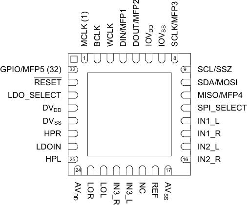
Pin Functions
| PIN | NAME | TYPE(1) | DESCRIPTION | |
|---|---|---|---|---|
| 1 | MCLK | DI | Master Clock Input | |
| 2 | BCLK | DIO | Audio serial data bus (primary) bit clock | |
| 3 | WCLK | DIO | Audio serial data bus (primary) word clock | |
| 4 | DIN | DI | Primary function: | |
| Audio serial data bus data input | ||||
| MFP1 | Secondary function: | |||
| General Purpose Clock Input General Purpose Input |
||||
| 5 | DOUT | DO | Primary function: | |
| Audio serial data bus data output | ||||
| MFP2 | Secondary function: | |||
| General Purpose Output Clock Output INT1 Output INT2 Output Audio serial data bus (secondary) bit clock output Audio serial data bus (secondary) word clock output |
||||
| 6 | IOVDD | Power | IO voltage supply 1.1V – 3.6V | |
| 7 | IOVSS | Ground | IO ground supply | |
| 8 | SCLK | DI | Primary function: (SPI_Select = 1) | |
| / | SPI serial clock | |||
| MFP3 | Secondary function: (SPI_Select = 0) | |||
| Audio serial data bus (secondary) bit clock input Audio serial data bus (secondary) DAC or common word clock input Audio serial data bus (secondary) ADC word clock input Audio serial data bus (secondary) data input General Purpose Input |
||||
| 9 | SCL/SS | DI | I2C interface serial clock (SPI_Select = 0) SPI interface mode chip-select signal (SPI_Select = 1) |
|
| 10 | SDA/MOSI | DI | I2C interface mode serial data input (SPI_Select = 0) SPI interface mode serial data input (SPI_Select = 1) |
|
| 11 | MISO | DO | Primary function: (SPI_Select = 1) | |
| / | Serial data output | |||
| MFP4 | Secondary function: (SPI_Select = 0) | |||
| General purpose output CLKOUT output INT1 output INT2 output Audio serial data bus (primary) ADC word clock output Audio serial data bus (secondary) data output Audio serial data bus (secondary) bit clock output Audio serial data bus (secondary) word clock output |
||||
| 12 | SPI_ SELECT | DI | Control mode select pin ( 1 = SPI, 0 = I2C ) | |
| 13 | IN1_L | AI | Multifunction Analog Input, or Single-ended configuration: Line 1 left or Differential configuration: Line right, negative |
|
| 14 | IN1_R | AI | Multifunction Analog Input, or Single-ended configuration: or Line 1 right or Differential configuration: Line right, positive |
|
| 15 | IN2_L | AI | Multifunction Analog Input, or Single-ended configuration: Line 2 left or Differential configuration: Line left, positive |
|
| 16 | IN2_R | AI | Multifunction Analog Input, or Single-ended configuration: Line 2 right or Differential configuration: Line left, negative |
|
| 17 | AVSS | Ground | Analog ground supply | |
| 18 | REF | AO | Reference voltage output for filtering | |
| 19 | NC | -- | NC, do not connect | |
| 20 | IN3_L | AI | Multifunction Analog Input, or Single-ended configuration: Line 3 left, or Differential configuration: Line left, positive, or Differential configuration: Line right, negative |
|
| 21 | IN3_R | AI | Multifunction Analog Input, or Single-ended configuration: Line 3 right, or Differential configuration: Line left, negative, or Differential configuration: Line right, positive |
|
| 22 | LOL | AO | Left line output | |
| 23 | LOR | AO | Right line output | |
| 24 | AVDD | Power | Analog voltage supply 1.5V–1.95V Input when A-LDO disabled, Filtering output when A-LDO enabled |
|
| 25 | HPL | AO | Left high power output driver | |
| 26 | LDOIN/HPVDD | Power | LDO Input supply and Headphone Power supply 1.9V– 3.6V | |
| 27 | HPR | AO | Right high power output driver | |
| 28 | DVSS | Ground | Digital Ground and Chip-substrate | |
| 29 | DVDD | Power | If LDO_SELECT Pin = 0 (D-LDO disabled) | |
| Digital voltage supply 1.26V – 1.95V | ||||
| If LDO_SELECT Pin = 1 (D-LDO enabled) | ||||
| Digital voltage supply filtering output | ||||
| 30 | LDO_ SELECT | DI | D-LDO enable signal (1 = D-LDO enable, 0 = D-LDO disabled) | |
| 31 | RESET | DI | Reset (active low) | |
| 32 | GPIO | DI | Primary function: | |
| General Purpose digital IO | ||||
| MFP5 | Secondary function: | |||
| CLKOUT Output INT1 Output INT2 Output Audio serial data bus ADC word clock output Audio serial data bus (secondary) bit clock output Audio serial data bus (secondary) word clock output |
||||
| Thermal Pad | Thermal Pad | N/A | Connect to PCB ground plane. Not internally connected. | |
(1) DI (Digital Input), DO (Digital Output), DIO (Digital Input/Output), AI (Analog Input), AO (Analog Output), AIO (Analog Input/Output)