SBOS708B May   2016  – August 2016 REF6025 , REF6030 , REF6033 , REF6041 , REF6045 , REF6050

PRODUCTION DATA.  

  1. Features
  2. Applications
  3. Description
    1.     Device Images
      1.      Typical Application
      2.      Reference Droop comparison (1 LSB = 19.07 µV, With ADS8881 at 1 MSPS)
  4. Revision History
  5. Device Comparison Table
  6. Pin Configuration and Functions
    1.     Pin Functions
  7. Specifications
    1. 7.1 Absolute Maximum Ratings
    2. 7.2 ESD Ratings
    3. 7.3 Recommended Operating Conditions
    4. 7.4 Thermal Information
    5. 7.5 Electrical Characteristics
    6. 7.6 Typical Characteristics
  8. Parameter Measurement Information
    1. 8.1 Solder Heat Shift
    2. 8.2 Thermal Hysteresis
    3. 8.3 Reference Droop Measurements
    4. 8.4 1/f Noise Performance
  9. Detailed Description
    1. 9.1 Overview
    2. 9.2 Functional Block Diagram
    3. 9.3 Feature Description
      1. 9.3.1 Integrated ADC Drive Buffer
      2. 9.3.2 Temperature Drift
      3. 9.3.3 Load Current
      4. 9.3.4 Stability
    4. 9.4 Device Functional Modes
  10. 10Applications and Implementation
    1. 10.1 Application Information
    2. 10.2 Typical Application
      1. 10.2.1 Design Requirements
      2. 10.2.2 Detailed Design Procedure
        1. 10.2.2.1 Results
      3. 10.2.3 Application Curves
  11. 11Power Supply Recommendations
  12. 12Layout
    1. 12.1 Layout Guidelines
    2. 12.2 Layout Example
  13. 13Device and Documentation Support
    1. 13.1 Documentation Support
      1. 13.1.1 Related Documentation
    2. 13.2 Related Links
    3. 13.3 Receiving Notification of Documentation Updates
    4. 13.4 Community Resources
    5. 13.5 Trademarks
    6. 13.6 Electrostatic Discharge Caution
    7. 13.7 Glossary
  14. 14Mechanical, Packaging, and Orderable Information

Package Options

Mechanical Data (Package|Pins)
Thermal pad, mechanical data (Package|Pins)
Orderable Information

Power Supply Recommendations

The REF60xx family of references have extremely low dropout voltage. The dropout specifications can be found in the Electrical Characteristics section. A minimum 0.1 µF decoupling capacitor must be connected between the VIN and GND_F pins of the REF60xx. A typical dropout voltage versus load is shown in Figure 61.
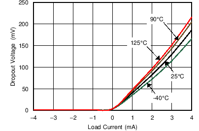
REF6025 REF6030 REF6033 REF6041 REF6045 REF6050 C017_SBOS708.png
Figure 61. Dropout Voltage vs Load Current