SBOS748 September   2016 REF6225 , REF6230 , REF6233 , REF6241 , REF6245 , REF6250

PRODUCTION DATA.  

  1. Features
  2. Applications
  3. Description
    1.     Device Images
      1.      Typical Application
      2.      Reference Droop comparison (1 LSB = 19.07 µV, With ADS8881 at 1 MSPS)
  4. Revision History
  5. Device Comparison Table
  6. Pin Configuration and Functions
    1.     Pin Functions
  7. Specifications
    1. 7.1 Absolute Maximum Ratings
    2. 7.2 ESD Ratings
    3. 7.3 Recommended Operating Conditions
    4. 7.4 Thermal Information
    5. 7.5 Electrical Characteristics
    6. 7.6 Typical Characteristics
  8. Parameter Measurement Information
    1. 8.1 Solder Heat Shift
    2. 8.2 Thermal Hysteresis
    3. 8.3 Reference Droop Measurements
    4. 8.4 1/f Noise Performance
  9. Detailed Description
    1. 9.1 Overview
    2. 9.2 Functional Block Diagram
    3. 9.3 Feature Description
      1. 9.3.1 Integrated ADC Drive Buffer
      2. 9.3.2 Temperature Drift
      3. 9.3.3 Load Current
      4. 9.3.4 Stability
    4. 9.4 Device Functional Modes
  10. 10Applications and Implementation
    1. 10.1 Application Information
    2. 10.2 Typical Application
      1. 10.2.1 Design Requirements
      2. 10.2.2 Detailed Design Procedure
        1. 10.2.2.1 Results
      3. 10.2.3 Application Curves
  11. 11Power Supply Recommendations
  12. 12Layout
    1. 12.1 Layout Guidelines
    2. 12.2 Layout Example
  13. 13Device and Documentation Support
    1. 13.1 Documentation Support
      1. 13.1.1 Related Documentation
    2. 13.2 Related Links
    3. 13.3 Receiving Notification of Documentation Updates
    4. 13.4 Community Resources
    5. 13.5 Trademarks
    6. 13.6 Electrostatic Discharge Caution
    7. 13.7 Glossary
  14. 14Mechanical, Packaging, and Orderable Information

Package Options

Mechanical Data (Package|Pins)
Thermal pad, mechanical data (Package|Pins)
Orderable Information

1/f Noise Performance

Typical 0.1-Hz to 10-Hz voltage noise for the REF6225 is shown in Figure 46. The 1/f noise scales with output voltage, but remains 3 µVPP/V for all the variants. Peak-to-peak noise measurement setup is shown in Figure 47.
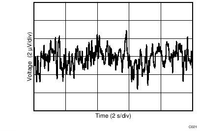
REF6225 REF6230 REF6233 REF6241 REF6245 REF6250 C021_SBOS708.pngFigure 46. 0.1-Hz to 10-Hz Noise
REF6225 REF6230 REF6233 REF6241 REF6245 REF6250 Noise_setup_REF62xx_BOS748.gifFigure 47. 0.1-Hz to 10-Hz Noise Measurement Setup