SDLS032H December 1983 – September 2016 SN5407 , SN5417 , SN7407 , SN7417
PRODUCTION DATA.
- 1 Features
- 2 Applications
- 3 Description
- 4 Revision History
- 5 Pin Configuration and Functions
- 6 Specifications
- 7 Parameter Measurement Information
- 8 Detailed Description
- 9 Application and Implementation
- 10Power Supply Recommendations
- 11Layout
- 12Device and Documentation Support
- 13Mechanical, Packaging, and Orderable Information
Package Options
Refer to the PDF data sheet for device specific package drawings
Mechanical Data (Package|Pins)
- J|14
- FK|20
- W|14
Thermal pad, mechanical data (Package|Pins)
Orderable Information
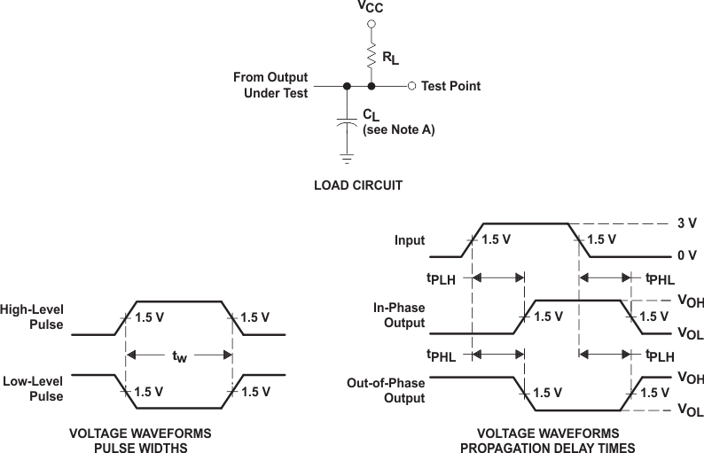
7 Parameter Measurement Information

A. CL includes probe and jig capacitance.
B. In the examples above, the phase relationships between inputs and outputs have been chosen arbitrarily.
C. All input pulses are supplied by generators having the following characteristics: PRR ≤ 1 MHz, ZO = 50 Ω, tr ≤ 7 ns,
tf ≤ 7 ns.
tf ≤ 7 ns.
D. The outputs are measured one at a time, with one input transition per measurement.
Figure 2. Load Circuit and Voltage Waveforms