SDLS025D December 1983 – May 2017 SN5400 , SN54LS00 , SN54S00 , SN7400 , SN74LS00 , SN74S00
PRODUCTION DATA.
- 1 Features
- 2 Applications
- 3 Description
- 4 Revision History
- 5 Pin Configuration and Functions
-
6 Specifications
- 6.1 Absolute Maximum Ratings
- 6.2 ESD Ratings: SN74LS00
- 6.3 Recommended Operating Conditions
- 6.4 Thermal Information
- 6.5 Electrical Characteristics: SNx400
- 6.6 Electrical Characteristics: SNx4LS00
- 6.7 Electrical Characteristics: SNx4S00
- 6.8 Switching Characteristics: SNx400
- 6.9 Switching Characteristics: SNx4LS00
- 6.10 Switching Characteristics: SNx4S00
- 6.11 Typical Characteristics
- 7 Parameter Measurement Information
- 8 Detailed Description
- 9 Application and Implementation
- 10Power Supply Recommendations
- 11Layout
- 12Device and Documentation Support
- 13Mechanical, Packaging, and Orderable Information
Package Options
Refer to the PDF data sheet for device specific package drawings
Mechanical Data (Package|Pins)
- J|14
- FK|20
- W|14
Thermal pad, mechanical data (Package|Pins)
Orderable Information
9 Application and Implementation
NOTE
Information in the following applications sections is not part of the TI component specification, and TI does not warrant its accuracy or completeness. TI’s customers are responsible for determining suitability of components for their purposes. Customers should validate and test their design implementation to confirm system functionality.
9.1 Application Information
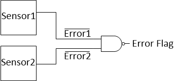
The SNx4xx00 devices are quadruple, 2-input NAND gate. A typical application of NAND gate can be as an error indicator as shown in Figure 3. If either of the sensor has an error, the error flag is high to indicate system error.
9.2 Typical Application
 Figure 3. Typical Application Diagram
9.2.1 Design Requirements
These devices use BJT technology and have unbalanced output drive with IOL and IOH specified as per the Recommended Operating Conditions.
9.2.2 Detailed Design Procedure
- Recommended Input Conditions:
- The inputs are TTL compliant.
- Because the base-emitter junction at the inputs breaks down, no voltage greater than 5.5 V must be applied to the inputs.
- Specified high and low levels: See VIH and VIL in Recommended Operating Conditions.
- Recommended Output Conditions:
- No more than one output must be shorted at a time as per the Electrical Characteristics: SNx400 for thermal stability and reliability.
- For high-current applications, consider thermal characteristics of the package listed in Thermal Information.
9.2.3 Application Curve
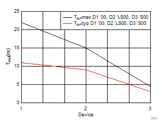
CL = 15 pF Figure 4. TPLH (Across Devices)