SLLSFC4 July 2019 SN65C1168E-SEP
PRODUCTION DATA.
- 1 Features
- 2 Applications
- 3 Description
- 4 Revision History
- 5 Pin Configuration and Functions
- 6 Specifications
- 7 Parameter Measurement Information
- 8 Detailed Description
- 9 Application and Implementation
- 10Power Supply Recommendations
- 11Device and Documentation Support
- 12Mechanical, Packaging, and Orderable Information
Package Options
Mechanical Data (Package|Pins)
- PW|16
Thermal pad, mechanical data (Package|Pins)
Orderable Information
9.1 Application Information
Figure 7 shows a typical RS-422 application. One transmitter is able to broadcast to multiple receiving nodes connected together over a shared differential bus. Twisted-pair cabling with a controlled differential impedance is used, and a termination resistance is placed at the farthest receive end of the cable in order to match the transmission line impedance and minimize signal reflections.
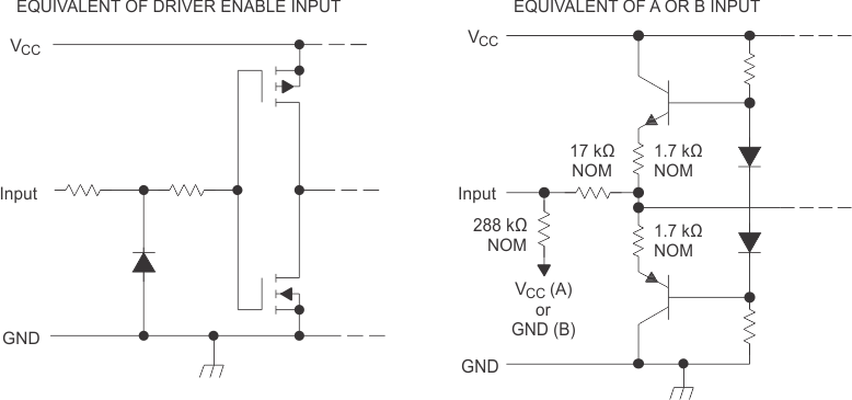
 Figure 7. Schematic of Inputs
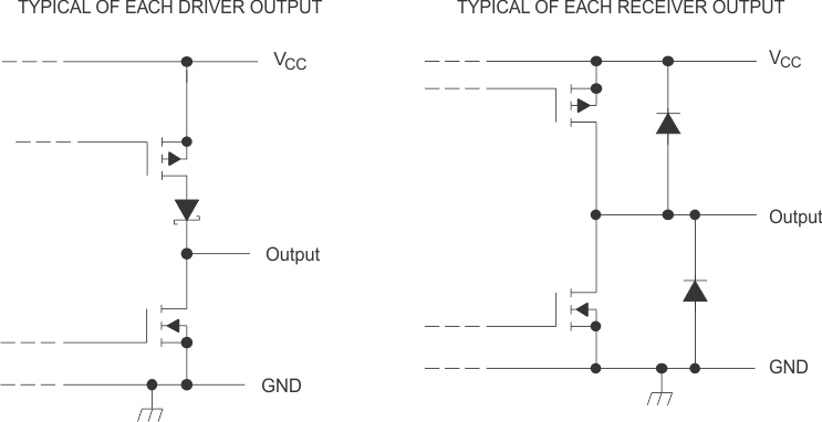
  Figure 8. Schematic of Outputs