SLLSFC4 July 2019 SN65C1168E-SEP
PRODUCTION DATA.
- 1 Features
- 2 Applications
- 3 Description
- 4 Revision History
- 5 Pin Configuration and Functions
- 6 Specifications
- 7 Parameter Measurement Information
- 8 Detailed Description
- 9 Application and Implementation
- 10Power Supply Recommendations
- 11Device and Documentation Support
- 12Mechanical, Packaging, and Orderable Information
Package Options
Mechanical Data (Package|Pins)
- PW|16
Thermal pad, mechanical data (Package|Pins)
Orderable Information
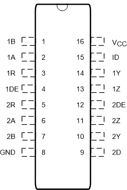
5 Pin Configuration and Functions
PW Package
16-Pin TSSOP
Top View

Pin Functions
| PIN | I/O | DESCRIPTION | |||
|---|---|---|---|---|---|
| NAME | NO. | ||||
| 1A | 2 | I | RS422 differential input (noninverting) to receiver 1 | ||
| 2A | 6 | I | RS422 differential input (noninverting) to receiver 2 | ||
| 1B | 1 | I | RS422 differential input (inverting) to receiver 1 | ||
| 2B | 7 | I | RS422 differential input (inverting) to receiver 2 | ||
| 1D | 15 | I | Logic data input to RS422 driver 1 | ||
| 2D | 9 | I | Logic data input to RS422 driver 2 | ||
| 1DE | 4 | I | Driver 1 enable (active high) | ||
| 2DE | 12 | I | Driver 2 enable (active high) | ||
| GND | 8 | — | Device ground | ||
| 1R | 3 | O | Logic data output of RS422 receiver 1 | ||
| 2R | 5 | O | Logic data output of RS422 receiver 2 | ||
| VCC | 16 | — | Power supply | ||
| 1Y | 14 | O | RS-422 differential (noninverting) driver output 1 | ||
| 2Y | 10 | O | RS-422 differential (noninverting) driver output 2 | ||
| 1Z | 13 | O | RS-422 differential (noninverting) driver output 1 | ||
| 2Z | 11 | O | RS-422 differential (noninverting) driver output 2 | ||