SLLSEJ8E June 2014 – April 2019 SN65HVD1470 , SN65HVD1471 , SN65HVD1473 , SN65HVD1474 , SN65HVD1476 , SN65HVD1477
PRODUCTION DATA.
- 1 Features
- 2 Applications
- 3 Description
- 4 Revision History
- 5 Device Comparison Table
- 6 Pin Configuration and Functions
-
7 Specifications
- 7.1 Absolute Maximum Ratings
- 7.2 ESD Ratings
- 7.3 Recommended Operating Conditions
- 7.4 Thermal Information — D Packages
- 7.5 Thermal Information — DGS and DGK Packages
- 7.6 Power Dissipation
- 7.7 Electrical Characteristics
- 7.8 Switching Characteristics — 400 kbps
- 7.9 Switching Characteristics — 20 Mbps
- 7.10 Switching Characteristics — 50 Mbps
- 7.11 Typical Characteristics
- 8 Parameter Measurement Information
- 9 Detailed Description
- 10Application and Implementation
- 11Power Supply Recommendations
- 12Layout
- 13Device and Documentation Support
- 14Mechanical, Packaging, and Orderable Information
Package Options
Mechanical Data (Package|Pins)
Thermal pad, mechanical data (Package|Pins)
Orderable Information
10.1 Application Information
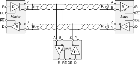
The SN65HVD147x family consists of full-duplex RS-485 transceivers commonly used for asynchronous data transmissions. Full-duplex implementation requires two signal pairs (four wires), and allows each node to transmit data on one pair while simultaneously receiving data on the other pair.
To eliminate line reflections, each cable end is terminated with a termination resistor, R(T), whose value matches the characteristic impedance, Z0, of the cable. This method, known as parallel termination, allows for higher data rates over longer cable length.
 Figure 30. Typical RS-485 Network With SN65HVD147x Full-Duplex Transceivers