SLLS612F June 2004 – February 2023 SN65HVD485E
PRODUCTION DATA
- 1 Features
- 2 Applications
- 3 Description
- 4 Revision History
- 5 Device Comparison Table
- 6 Pin Configuration and Functions
-
7 Specifications
- 7.1 Absolute Maximum Ratings
- 7.2 ESD Ratings
- 7.3 Recommended Operating Conditions
- 7.4 Thermal Information
- 7.5 Electrical Characteristics: Driver
- 7.6 Electrical Characteristics: Receiver
- 7.7 Power Dissipation Characteristics
- 7.8 Supply Current
- 7.9 Switching Characteristics: Driver
- 7.10 Switching Characteristics: Receiver
- 7.11 Dissipation Ratings
- 7.12 Typical Characteristics
- 8 Detailed Description
- 9 Application and Implementation
- 10Device and Documentation Support
- 11Mechanical, Packaging, and Orderable Information
Package Options
Mechanical Data (Package|Pins)
Thermal pad, mechanical data (Package|Pins)
Orderable Information
8.4 Device Functional Modes
When the driver enable pin (DE) is logic high, the differential outputs A and B follow the logic states at data input D. A logic high at D causes A to turn high and B to turn low. In this case, the differential output voltage defined as VOD = VA – VB is positive. When D is low, the output states reverse, B turns high, A is low, and VOD is negative.
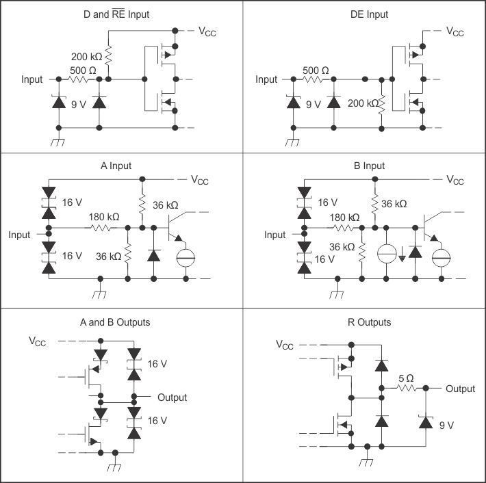
When DE is low, both outputs turn high impedance. In this condition, the logic state at D is irrelevant. The DE pin has an internal pulldown resistor to ground; thus when left open, the driver is disabled (high impedance) by default. The D pin has an internal pullup resistor to VCC; thus when left open while the driver is enabled, output A turns high and B turns low.
| INPUT D | ENABLE DE | OUTPUTS | FUNCTION | |
|---|---|---|---|---|
| A | B | |||
| H | H | H | L | Actively drive bus High |
| L | H | L | H | Actively drive bus Low |
| X | L | Z | Z | Driver disabled |
| X | OPEN | Z | Z | Driver disabled by default |
| OPEN | H | H | L | Actively drive bus high by default |
When the receiver enable pin ( RE) is logic low, the receiver is enabled. When the differential input voltage defined as VID = VA – VB is positive and higher than the positive input threshold (VIT+) the receiver output (R) turns high. When VID is negative and lower than the negative input threshold (VIT–), the receiver output (R) turns low. If VID is between VIT+ and VIT–, the output is indeterminate.
When RE is logic high or left open, the receiver output is high impedance and the magnitude and polarity of VID are irrelevant. Internal biasing of the receiver inputs causes the output to go failsafe high when the transceiver is disconnected from the bus (open-circuit), the bus lines are shorted (short-circuit), or the bus is not actively driven (idle bus).
| DIFFERENTIAL INPUT VID = VA – VB | ENABLE RE | OUTPUT R | FUNCTION |
|---|---|---|---|
| VIT+ < VID | L | H | Receive valid bus High |
| VIT– < VID < VIT+ | L | ? | Indeterminate bus state |
| VID < VIT– | L | L | Receive valid bus Low |
| X | H | Z | Receiver disabled |
| X | OPEN | Z | Receiver disabled by default |
| Open-circuit bus | L | H | Fail-safe high output |
| Short-circuit bus | L | H | Fail-safe high output |
| Idle (terminated) bus | L | H | Fail-safe high output |
 Figure 8-1 Equivalent Input and Output Schematic Diagrams