SLLS612F June 2004 – February 2023 SN65HVD485E
PRODUCTION DATA
- 1 Features
- 2 Applications
- 3 Description
- 4 Revision History
- 5 Device Comparison Table
- 6 Pin Configuration and Functions
-
7 Specifications
- 7.1 Absolute Maximum Ratings
- 7.2 ESD Ratings
- 7.3 Recommended Operating Conditions
- 7.4 Thermal Information
- 7.5 Electrical Characteristics: Driver
- 7.6 Electrical Characteristics: Receiver
- 7.7 Power Dissipation Characteristics
- 7.8 Supply Current
- 7.9 Switching Characteristics: Driver
- 7.10 Switching Characteristics: Receiver
- 7.11 Dissipation Ratings
- 7.12 Typical Characteristics
- 8 Detailed Description
- 9 Application and Implementation
- 10Device and Documentation Support
- 11Mechanical, Packaging, and Orderable Information
Package Options
Mechanical Data (Package|Pins)
Thermal pad, mechanical data (Package|Pins)
Orderable Information
3 Description
The SN65HVD485E device is a half-duplex transceiver designed for RS-485 data bus networks. Powered by a 5-V supply, it is fully compliant with the TIA/EIA-485A standard. This device is suitable for data transmission up to 10 Mbps over long twisted-pair cables and is designed to operate with very low supply current, typically less than 2 mA, exclusive of the load. When the device is in the inactive shutdown mode, the supply current drops below 1 mA.
The wide common-mode range and high ESD protection levels of this device make it suitable for demanding applications such as: electrical inverters, status/command signals across telecom racks, cabled chassis interconnects, and industrial automation networks where noise tolerance is essential. The SN65HVD485E device matches the industry-standard footprint of the SN75176 device. Power-on reset circuits keep the outputs in a high-impedance state until the supply voltage has stabilized. A thermal-shutdown function protects the device from damage due to system-fault conditions. The SN65HVD485E device is characterized for operation from –40°C to 85°C air temperature.
| PART NUMBER | PACKAGE(1) | BODY SIZE (NOM) |
|---|---|---|
| SN65HVD485E | SOIC (8) | 4.91 mm × 3.90 mm |
| VSSOP (8) | 3.00 mm × 3.00 mm | |
| PDIP (8) | 9.81 mm × 6.35 mm |
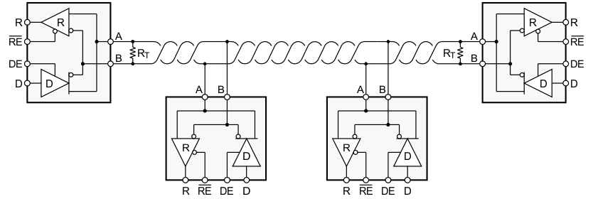
 Typical Application Schematic