SLLS261N July 1997 – April 2021 SN55LVDS31 , SN65LVDS31 , SN65LVDS3487 , SN65LVDS9638
PRODUCTION DATA
- 1 Features
- 2 Applications
- 3 Description
- 4 Revision History
- 5 Description (Continued)
- 6 Pin Configuration and Functions
-
7 Specifications
- 7.1 Absolute Maximum Ratings (1)
- 7.2 ESD Ratings
- 7.3 Recommended Operating Conditions
- 7.4 Thermal Information
- 7.5 Electrical Characteristics: SN55LVDS31
- 7.6 Electrical Characteristics: SN65LVDSxxxx
- 7.7 Switching Characteristics: SN55LVDS31
- 7.8 Switching Characteristics: SN65LVDSxxxx
- 7.9 Typical Characteristics
- 8 Parameter Measurement Information
- 9 Detailed Description
- 10Application and Implementation
- 11Power Supply Recommendations
- 12Layout
- 13Device and Documentation Support
- 14Mechanical, Packaging, and Orderable Information
Package Options
Refer to the PDF data sheet for device specific package drawings
Mechanical Data (Package|Pins)
- D|8
- DGK|8
- DGN|8
Thermal pad, mechanical data (Package|Pins)
Orderable Information
3 Description
The SN55LVDS31, SN65LVDS31, SN65LVDS3487, and SN65LVDS9638 devices are differential line drivers that implement the electrical characteristics of low-voltage differential signaling (LVDS). This signaling technique lowers the output voltage levels of 5-V differential standard levels (such as TIA/EIA-422B) to reduce the power, increase the switching speeds, and allow operation with a 3.3-V supply rail. Any of the four current-mode drivers will deliver a minimum differential output voltage magnitude of 247 mV into a 100-Ω load when enabled.
| PART NUMBER | PACKAGE | BODY SIZE (NOM) |
|---|---|---|
| SN55LVDS31 | LCCC (20) | 8.89 mm × 8.89 mm |
| CDIP (16) | 19.56 mm × 6.92 mm | |
| CFP (16) | 10.30 mm × 6.73 mm | |
| SN65LVDS31 | SOIC (16) | 9.90 mm × 3.91 mm |
| SOP (16) | 10.30 mm × 5.30 mm | |
| TSSOP (16) | 5.00 mm × 4.40 mm | |
| SN65LVDS3487 | SOIC (16) | 9.90 mm × 3.91 mm |
| TSSOP (16) | 5.00 mm × 4.40 mm | |
| SN65LVDS9638 | SOIC (8) | 4.90 mm × 3.91 mm |
| VSSOP (8) | 3.00 mm × 3.00 mm | |
| HVSSOP (8) | 3.00 mm × 3.00 mm |
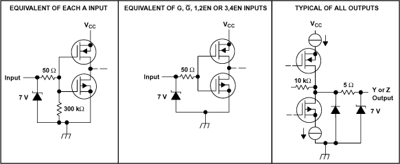
 Equivalent Input and Output Schematic Diagrams