SLLS261N July   1997  – April 2021 SN55LVDS31 , SN65LVDS31 , SN65LVDS3487 , SN65LVDS9638

PRODUCTION DATA  

  1. Features
  2. Applications
  3. Description
  4. Revision History
  5. Description (Continued)
  6. Pin Configuration and Functions
  7. Specifications
    1. 7.1 Absolute Maximum Ratings (1)
    2. 7.2 ESD Ratings
    3. 7.3 Recommended Operating Conditions
    4. 7.4 Thermal Information
    5. 7.5 Electrical Characteristics: SN55LVDS31
    6. 7.6 Electrical Characteristics: SN65LVDSxxxx
    7. 7.7 Switching Characteristics: SN55LVDS31
    8. 7.8 Switching Characteristics: SN65LVDSxxxx
    9. 7.9 Typical Characteristics
      1. 7.9.1 17
  8. Parameter Measurement Information
    1. 8.1 19
  9. Detailed Description
    1. 9.1 Overview
    2. 9.2 Functional Block Diagram
    3. 9.3 Feature Description
      1. 9.3.1 Driver Disabled Output
      2. 9.3.2 NC Pins
      3. 9.3.3 Unused Enable Pins
      4. 9.3.4 Driver Equivalent Schematics
    4. 9.4 Device Functional Modes
  10. 10Application and Implementation
    1. 10.1 Application Information
    2. 10.2 Typical Application
      1. 10.2.1 Point-to-Point Communications
        1. 10.2.1.1 Design Requirements
        2. 10.2.1.2 Detailed Design Procedure
          1. 10.2.1.2.1 Driver Supply Voltage
          2. 10.2.1.2.2 Driver Bypass Capacitance
          3. 10.2.1.2.3 Driver Output Voltage
          4. 10.2.1.2.4 Interconnecting Media
          5. 10.2.1.2.5 PCB Transmission Lines
          6. 10.2.1.2.6 Termination Resistor
          7. 10.2.1.2.7 Driver NC Pins
        3. 10.2.1.3 Application Curve
      2. 10.2.2 Multidrop Communications
        1. 10.2.2.1 Design Requirements
        2. 10.2.2.2 Detailed Design Procedure
          1. 10.2.2.2.1 Interconnecting Media
        3. 10.2.2.3 Application Curve
  11. 11Power Supply Recommendations
    1. 11.1 49
  12. 12Layout
    1. 12.1 Layout Guidelines
      1. 12.1.1 Microstrip vs. Stripline Topologies
      2. 12.1.2 Dielectric Type and Board Construction
      3. 12.1.3 Recommended Stack Layout
      4. 12.1.4 Separation Between Traces
      5. 12.1.5 Crosstalk and Ground Bounce Minimization
    2. 12.2 Layout Example
  13. 13Device and Documentation Support
    1. 13.1 Device Support
      1. 13.1.1 Other LVDS Products
    2. 13.2 Documentation Support
      1. 13.2.1 Related Information
      2. 13.2.2 Receiving Notification of Documentation Updates
      3. 13.2.3 Related Links
    3. 13.3 Support Resources
    4. 13.4 Trademarks
    5. 13.5 Electrostatic Discharge Caution
    6. 13.6 Glossary
  14. 14Mechanical, Packaging, and Orderable Information

Package Options

Refer to the PDF data sheet for device specific package drawings

Mechanical Data (Package|Pins)
  • D|8
  • DGK|8
  • DGN|8
Thermal pad, mechanical data (Package|Pins)
Orderable Information

Microstrip vs. Stripline Topologies

As per SLLD009, printed-circuit boards usually offer designers two transmission line options: Microstrip and stripline. Microstrips are traces on the outer layer of a PCB, as shown in Figure 12-1.
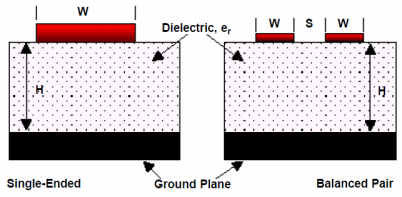
GUID-EB030F35-4B71-4561-8990-92F744EB7408-low.pngFigure 12-1 Microstrip Topology

On the other hand, striplines are traces between two ground planes. Striplines are less prone to emissions and susceptibility problems because the reference planes effectively shield the embedded traces. However, from the standpoint of high-speed transmission, juxtaposing two planes creates additional capacitance. TI recommends routing LVDS signals on microstrip transmission lines, if possible. The PCB traces allow designers to specify the necessary tolerances for ZO based on the overall noise budget and reflection allowances. Footnotes 11, 22, and 33 provide formulas for ZO and tPD for differential and single-ended traces. (2)(3)(4)
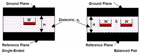
GUID-690DD262-BEFC-479D-ABC0-EECE8C9B1BF2-low.pngFigure 12-2 Stripline Topology
Howard Johnson & Martin Graham.1993. High Speed Digital Design – A Handbook of Black Magic. Prentice Hall PRT. ISBN number 013395724.
Mark I. Montrose. 1996. Printed Circuit Board Design Techniques for EMC Compliance. IEEE Press. ISBN number 0780311310.
Clyde F. Coombs, Jr. Ed, Printed Circuits Handbook, McGraw Hill, ISBN number 0070127549.