SDLS032H December 1983 – September 2016 SN5407 , SN5417 , SN7407 , SN7417
PRODUCTION DATA.
- 1 Features
- 2 Applications
- 3 Description
- 4 Revision History
- 5 Pin Configuration and Functions
- 6 Specifications
- 7 Parameter Measurement Information
- 8 Detailed Description
- 9 Application and Implementation
- 10Power Supply Recommendations
- 11Layout
- 12Device and Documentation Support
- 13Mechanical, Packaging, and Orderable Information
Package Options
Refer to the PDF data sheet for device specific package drawings
Mechanical Data (Package|Pins)
- D|14
- N|14
Thermal pad, mechanical data (Package|Pins)
Orderable Information
8 Detailed Description
8.1 Overview
The SN74x7 is a high sink current capable open-collector buffer. This device is high-voltage tolerant on the output of up to 30 V on the SNx407 model and 15 V on the SNx417 model. The SN74x7 is also useful for converting TTL voltage levels to MOS levels.
8.2 Functional Block Diagram

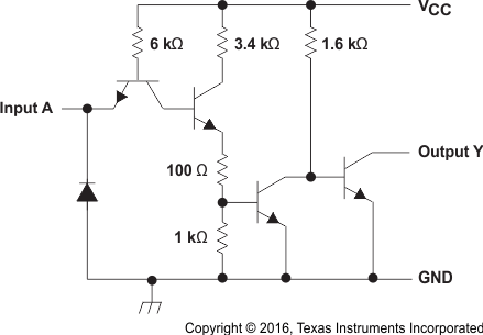
Resister values shown are nominal.
Figure 3. Schematic
8.3 Feature Description
The SNx407 and SNx417 devices are ideal for high voltage outputs. The SNx407 device has a maximum output voltage 30 V and the SNx417 device has a maximum output voltage 15 V.
The high sink current is up to 40 mA for the SN74x7.
8.4 Device Functional Modes
Table 1 lists the functions of the devices.